Download
1 / 19
190 likes | 329 Views
Microprocessor-based systems. Course 6 Memory design. bk. b1. b0. 0. 1. 2. bk. b1. b0. l-1. columns. 0. 1. 2. c-1. addresses. locations. 0. 1. Lines. location. 2. n-1. Linear structure. Matrix structure. Memory circuits. Memory cell:

E N D
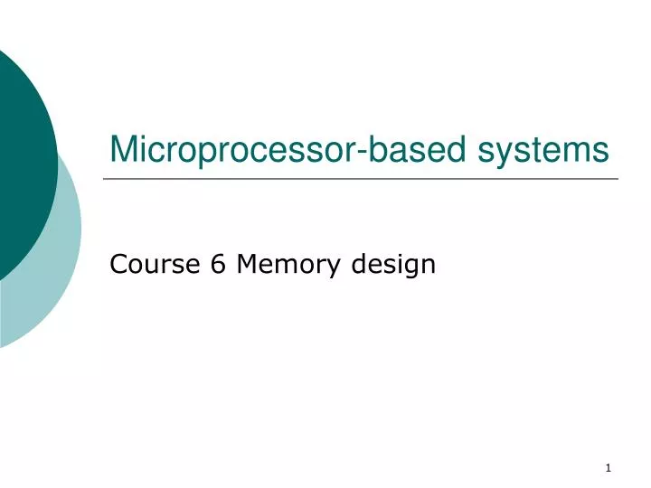
Microprocessor-based systems Course 6 Memory design
bk . . . b1 b0 0 1 . . . 2 . . . . bk . . . b1 b0 . . . . l-1 columns 0 1 2 . . c-1 addresses locations 0 1 Lines location 2 . . . n-1 Linear structure Matrix structure Memory circuits • Memory cell: • A digital circuit that memorize one bit (e.g.: flip-flop) • Memory location (memory word) • Set of elementary memory cells accessed (read or written) simultaneously • The basic addressing element (1, 4, 8,16, 32 bits) • Every location has an address • Memory circuit = Set of memory locations • Memory capacity – total number of locations (addresses)
Characteristics of a memory circuit • Geometry of internal organization: • The length of the memory word, organization and addressing. • Memory capacity, • Expressed in number of memory locations or in bytes • For example:32 kbytes,64 kB, 256MB, 1GB. • Volatility: loss of data • ROM memory (Read Only Memories) – keeps/stores the data even when the power supply is switched off • ROM, PROM, EPROM, EEPROM, Flash • RAM memory (Random Access Memories): it looses its content if the power supply is switched off • Static RAM (SRAM) • High speed, low capacity • Dynamic RAM (DRAM): it looses its memory in time • Medium speed, very high capacity
Characteristics of a memory circuit • Memory technologies: • bipolar (TTL, TTL Shottky, ECL) – fast but low integration ratio, high power consumption • MOS, CMOS – high integration ratio, high capacity, average speed, small power consumption • Time features: • Access time: the time needed to read or write a memory location; expressed in nanoseconds [ns]. • The duration of a read or write cycle • The memory’s speed determined by its access time or transfer cycle • Power consumption, expressed in w/bit. • Bipolar memories have higher power consumption; it depends on the capacity • MOS memories have very low power consumption; it depends on the access frequency
ADDR DEC A0 ADDR Valid Address A1 tCS CS tOE OE An DATA Valid Data Control logic CS Data Amplifiers for read and programming tACC tOH PROG TCYCLE OE Dk Dk-1 D0 D1 a. b. Non-volatile memories: ROM, PROM EPROM, EEPROM, Flash • The internal structure of a ROM memory
T WL Vcc WL T1 WL F PL T DL DL T2 DL PROM EPROM ROM Non-volatile memories: ROM, PROM EPROM, EEPROM, Flash • ROM – Cannot be written, only read operations are allowed • Written by the producer (through masks) • PROM – Programmable ROM -One write (programming) operation is allowed for the used • EPROM (UV) – Erasable PROM – a limited number of erase and re-write operations are allowed (aprox. 100 cycles) • EEPROM– Electrically EPROM – electrical erase and re-write (aprox. 100.000 cycles) • Flash – type of EEPROM with a block organization and higher capacity
Static RAM memories TCITIRE ADDR DEC ADDR Valid address A0 Memory matrix tCD A1 CS R/W “1” DATA Valid Data An-1 tACC Input amplifier Output amplifier b1. TSCRIERE k k Control logic CS ADDR Valid address Input/output circuit WR CS R/W Dk-2 D0 Dk-1 D1 DATA Valid Data Internal structure tDM Time diagrams for read and write operations
ID k-1 ID 1 ID 0 Q Q Q D D D C C C Q Q Q D D D C C C Q Q Q D D D C C C ADDR DEC A0 A1 An-1 CS R/W OD 1 OD k-1 OD 0 Structure of RAM memory
WL/W 0 1 2 . . 2n/2-1 0 1 2 Raw addr. dec . . 2n/2-1 WL/R Raw address reg RAS n/2 T2 T1 A0 A1 Column address reg MUX / DMUX 2n/2-1:1 / 1: 2n/2-1 WE T3 An/2-1 n/2 n/2 C DL ID OD CAS Dynamic RAM memory • The elementary memory cell is a condenser • It is charged (logical 1) or not (logical 0) at write operation; • The charge is lost in time (in aprox. 2 ms) • High capacity • Requires refresh operations DRAM Memory cell
TREAD TWRITE ADDR ADDR Raw addr Raw addr Column addr. Column addr. RAS RAS CAS CAS WE WE Valid data DATA DATA Valod data Read cycle Write cycle Trefresh ADDR Raw addr RAS CAS WE Refresh cycle Read, write and refresh cycles for DRAM memory
Design of a static RAM memory module • The structure of a memory module Selection Addresses Metrix of memory circuites Data Address Amp. Data Amp. Module selection Control circuit Dec Commands
Design parameters • Memory capacity (KB, MB) • Internal organization (ex: 8, 16, 32 bits) • The bus: • Address lines, data lines and commands • Time restrictions • Start address (the module’s place in the addressing space of the processor) • Type of available memory circuits • Other functional requirements
Design steps • Building of a memory sub-module with the required data width • Build the memory matrix with the required capacity, using the previously built sub-modules • Design the decoder module • Design of address amplifiers • Design of data amplifiers • Design of the control circuit (if needed)
Design example • Capacity: 1Mbytes • Organization: 16 bits with access on 8 bits too • The bus: • ISA (24 address lines, 16 data lines, MRDC, MWTC) • Start address: C0000H • Available circuits: 64Kbytes
A1 A2 D0 64K*8 D1 A16 D7 WR\ CSLi\ D8 64K*8 D9 D15 CSHi\ Submodule 64K*16= 128K*8 Building a sub-module with the required data width
A1-A16 64K*16 D0-D15 WR\ CSL0\ CSH0\ 64K*16 CSL1\ CSH1\ … 64K*16 CSL7\ 512K*16=1M*8 CSH7\ Building the memory matrix with the required capacity
Design of the decoder unit A17-A23 CS0\ DEC DEC CS1\ CS7\ MRDC\, MWTC\ SelMod\ BHE\ A0 A23 CSL0\ A17 74LS138 A22 A18 A21 A19 CSH0\ A20 CSL7\ MRDC\ MWTC\ CSH7\ SelMod\
Design of address and data amplifiers SA0 A0 74LS244 SA1 A1 SA7 A7 SD0 D0 74LS245 SD1 D1 SD7 D7 RD\ SelMod\ SA8 A8 SA9 A9 74LS244 SA15 A15 SD8 D8 74LS245 SD9 D9 SD15 D15 SA16 A16 74LS244 SA23 A23