Download
1 / 19
190 likes | 197 Views
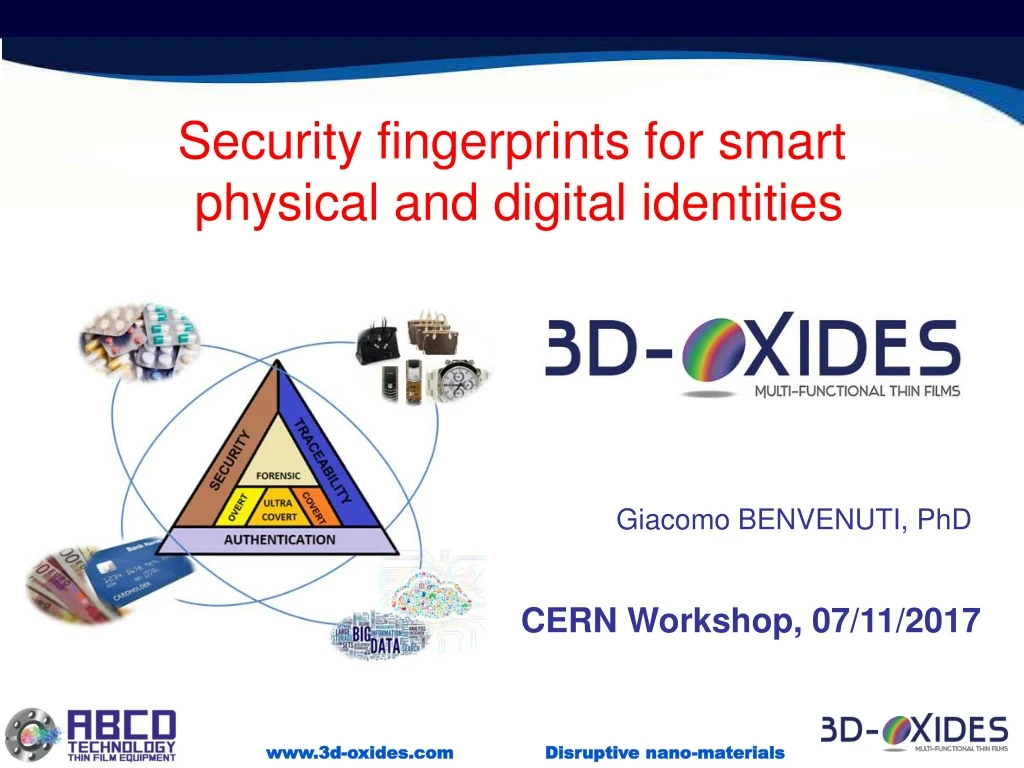
Security fingerprints for smart physical and digital identities. Giacomo BENVENUTI, PhD. CERN Workshop, 07/11/2017. Challenge: towards a smart 4.0 era. MANUFACTURING 4.0. SMART GRIDS. MOBILITY 4.0. 3D-PRINTING. INSURETECH. IoT & IIoT. SMART CITIES. SMART SERVICES. FINTECH.

E N D
Security fingerprints for smart physical and digital identities Giacomo BENVENUTI, PhD CERN Workshop, 07/11/2017
Challenge: towards a smart 4.0 era MANUFACTURING 4.0 SMART GRIDS MOBILITY 4.0 3D-PRINTING INSURETECH IoT & IIoT SMART CITIES SMART SERVICES FINTECH SUPPLY CHAINS BLOCKCHAIN + AI The 4th industrial revolution is here! Smart, Reliable & Intelligent objects.
Pains and hopes… Strong issues: Growing counterfeiting Weak cyber-security Poor traceability of objects and data Lack of trust and value managementBlockchains approachReinforced trust Improved interactions between: ≠ verticals ≠ partnersBut still too many technical intrinsic limits…
Physical and digital FINGERPRINTS Identities to make object SMART! Single object identities Mass Production Physical + Digital solution Strong miniaturization Affordable costs Experimental vs model
Our expertise. Micro and nano 3D and 4D-printing of multifunctional thin films materials
Thin films FUNCTIONALITY2 FUNCTIONALITY 1 PROPERTY 2 PROPERTY 1 + PATTERNING 2 + PATTERNING 1 + LAYER 2 + LAYER 1 SUBSTRATE A high-tech paint with dimensions of 10 nm to 10 mm allowing: • Miniaturization of devices • Development of new material properties due to nano-size effects • Integration of new functionalities (value) onto a substrate HIGH ADDED VALUE More (functionalities / value / quality of life) with less(resources / eco-impact ) = Sustainability
Markets & Applications of thin films PERVASIVE COST EFFECTIVE MASS PRODUCTION Less Resources, Robust devices, Transportability
Our additive growth set-ups Stencil-mask assisted deposition Deposition on patterned substrates 3 Laser-assisted deposition Chemicals under vacuum Mask
Mask Deposition DEPOSIT AFM MEASUREMENT: 1 mm 5 mm 32 nm 0 nm MATHEMATICAL DEPOSIT SIMULATION: DEPOSIT AFM MEASUREMENT: 142 nm 5 mm 0 nm MATHEMATICAL DEPOSIT SIMULATION: 5 mm
The 4th dimension… ≠ fingerprints vs external conditions. A cryptographic key…
Cryptography functionality 9 A first wavelength w1 is shined onto the e-tag on position (x,y). A second wavelength w2 is used to shine the e-tag on same positions (x,y) Checking of I2 values authenticates information provided by main tag. The first wavelength w1 is used to shine the e-tag on (x,y) position. 1 4 8 10 3 2 5 7 11 Alphanumeric character # is associated to light intensities value fingerprint (x, y, I1). (x ,y , #) (x ,y , I1) Light intensities values I2 associated to the tag fingerprint (x, y, I2) are recorded. I2 values are totally de-correlated from I1 The second wavelength w2 is used to shine the twin e-tag on (x,y) The message is decrypted (x, y, I1) (x, y, #) 6 TWIN TAG MAIN TAG Encrypted information (x, y, I2) is transferred
Other properties available… 0 5 10 15 20 25 30 Most material properties can be modulated and patterned.
≠ LEDs Our thin film acts as a tunable color filter as a function of the wavelength. Readers External reader Integrated reader
Benchmarking Digital World Quantum cryptography Software PUF Digital 3D-Tag Physical World Better and cheaper than competitors solutions
TRL Roadmap • Equipments Available for small series • Physical ID Addressing industrial PoC • Digital ID Addressing Lab PoC • Mass Production Easy equipment upgrading Most experimental incertitude addressed Need to optimize the production process
Conclusions All competitors functionalities PhysicalDigital Overt Firewall Covert PW generators Forensic Physical Unclonable Functions Ultra-covert Cryptography Monolithically IntegratedCMOS compatible productionNew Blockchain and AI models enabled
Outlook Looking for partners: Industries / R&D Labs Co-developers Integrators Early adopters (Industrial) Venture funds Production (2 M€) Marketing + sales (3M €)
Phone : +41-(0)78 82 39 839 +33-(0)7 777 54 397 giacomo.benvenuti@abcd-technology.com Thank youfor your attention.