Download
1 / 23
230 likes | 238 Views
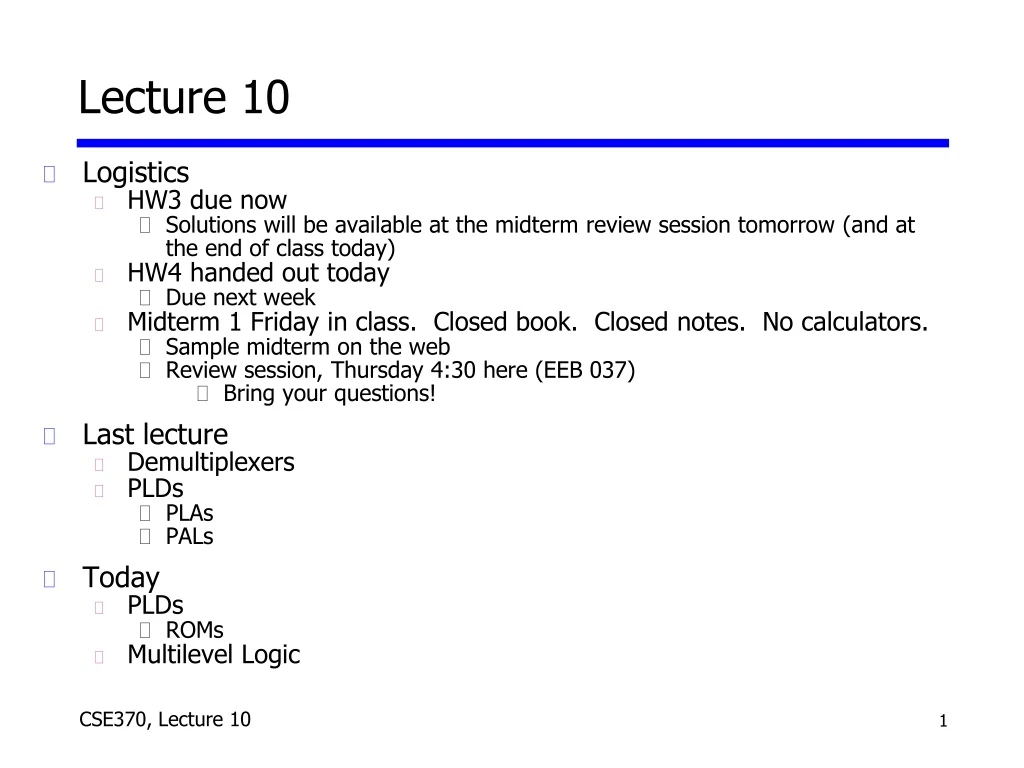
Lecture 10. Logistics HW3 due now Solutions will be available at the midterm review session tomorrow (and at the end of class today) HW4 handed out today Due next week Midterm 1 Friday in class. Closed book. Closed notes. No calculators. Sample midterm on the web

E N D
Lecture 10 • Logistics • HW3 due now • Solutions will be available at the midterm review session tomorrow (and at the end of class today) • HW4 handed out today • Due next week • Midterm 1 Friday in class. Closed book. Closed notes. No calculators. • Sample midterm on the web • Review session, Thursday 4:30 here (EEB 037) • Bring your questions! • Last lecture • Demultiplexers • PLDs • PLAs • PALs • Today • PLDs • ROMs • Multilevel Logic
Midterm 1 Topics Covered • Combinational logic basics • Binary/hex/decimal numbers • Ones and twos complement arithmetic • Truth tables • Boolean algebra • Basic logic gates • Schematic diagrams • de Morgan's theorem • AND/OR to NAND/NOR logic conversion • K-maps (up to 4 variables), logic minimization, don't cares • SOP, POS • Minterm and maxterm expansions (canonical, minimized)
Midterm 1 Topics Covered (continued) • Combinational logic applications • Combinational design • Input/output encoding • Truth table • K-map • Boolean equations • Schematics • Multiplexers
Recall example: BCD to Gray --- Wiring of a PLA A B C D W X Y Z Minimized functions: W = A + BC + BD X = BC' Y = B + C Z = A'B'C'D + BCD + AD' + B'CD'
Recall: Wiring a PAL Minimized functions: W = A + BC + BD X = BC' Y = B + C Z = A'B'C'D + BCD + AD' + B'CD’ Fine example for the use of PAL (because no shared AND terms) Many AND gates wasted, but still faster and cheaper than PLA
Compare implementations for this example • PLA: • No shared logic terms in this example • 10 decoded functions (10 AND gates) • PAL: • Z requires 4 product terms • 16 decoded functions (16 AND gates) • 6 unused AND gates • This decoder is a good candidate for PALs • 10 of 16 possible inputs are decoded • No sharing among AND terms • Another option? • Yes — a ROM
Read-only memories (ROMs) • Two dimensional array of stored 1s and 0s • Input is an address ROM decodes all possible input addresses • Stored row entry is called a "word" • ROM output is the decoded word n address lines • • • inputs memoryarray(2n wordsby m bits) 2n wordlines decoder outputs • • •
Like this special PLA example: only more efficient F1 = ABC F2 = A + B + C F3 = A' B' C' F4 = A' + B' + C' F5 = A xor B xor C F6 = A xnor B xnor C A B C A'B'C' A'B'C A'BC' A'BC AB'C' AB'C ABC' ABC F1 F2 F3 F4 F5 F6 Think of as a memory-address decoder 0 1 0 Memory bits 0 1 0 1 1 A B C F1 F2 F3 F4 F5 F6 0 0 0 0 0 1 1 0 0 0 0 1 0 1 0 1 1 1 0 1 0 0 1 0 1 1 1 0 1 1 0 1 0 1 0 0 1 0 0 0 1 0 1 1 1 1 0 1 0 1 0 1 0 0 1 1 0 0 1 0 1 0 0 1 1 1 1 1 0 0 1 1
ROM details • Similar to a PLA but with a fully decoded and fixed AND array • Completely flexible OR array (unlike a PAL) • Extremely dense: One transistor per stored bit +5V Only one word line is active at any time n-1 2 2 decoder 1 0 n-1 0 Address m-1 0 Outputs Bit lines: Normally pulled high through resistor. If transistor stores a zero, then line pulls low when row is selected
Two-level combinational logic using a ROM • Use a ROM to directly store a truth table • No need to minimize logic • Example: F0 = A'B'C + AB'C' + AB'C • F1 = A'B'C + A'BC' + ABC • F2 = A'B'C' + A'B'C + AB'C' • F3 = A'BC + AB'C' + ABC' A B C F0 F1 F2 F3 0 0 0 0 0 1 00 0 1 1 1 1 00 1 0 0 1 0 00 1 1 0 0 0 1 1 0 0 1 0 1 1 1 0 1 1 0 0 0 1 1 0 0 0 0 1 1 1 1 0 1 0 0 You specify whether to store 1 or 0 in each location in the ROM ROM8 words x 4 bits/word A B C F0 F1 F2 F3 address outputs
ROMs versus PLAs/PALs • ROMs • Benefits • Quick to design, simple, dense • Limitations • Size doubles for each additional input • Can't exploit don't cares • PLAs/PALs • Benefits • Logic minimization reduces size • PALs faster/cheaper than PLAs • Limitations • PAL OR-plane has hard-wired fan-in • Another alternative: Field programmable gate arrays • Learn a bit more later in this course
c0 c1 c5 c6 c4 c2 c3 Example: BCD to 7-segment display controller • The problem • Input is a 4-bit BCD digit (A, B, C, D) • Need signals to drive a display (7 outputs C0 – C6) c0 c1 c2 c3 c4 c5 c6 BCD to 7–segmentcontrol-signaldecoder A B C D
Formalize the problem • Truth table • Many don’t cares • Choose implementation target • If ROM, we are done • Don't cares imply PAL/PLA may be good choice • Implement design • Minimize the logic • Map into PAL/PLA A B C D C0 C1 C2 C3 C4 C5 C6 0 0 0 0 1 1 1 1 1 1 0 0 0 0 1 0 1 1 0 0 0 0 0 0 1 0 1 1 0 1 1 0 1 0 0 1 1 1 1 1 1 0 0 1 0 1 0 0 0 1 1 0 0 1 1 0 1 0 1 1 0 1 1 0 1 1 0 1 1 0 1 0 1 1 1 1 1 0 1 1 1 1 1 1 0 0 0 0 1 0 0 0 1 1 1 1 1 1 1 1 0 0 1 1 1 1 0 0 1 1 1 0 1 X X X X X X X X 1 1 X X X X X X X X X Not all rows of the truth table are listed separately
A A A A A A A 1 1 X 1 1 1 X 1 1 1 X X 0 1 X X 1 1 X 1 0 1 X 1 0 0 X X 0 1 X X 1 0 X 1 0 1 X 0 1 0 X X 1 1 X X 1 0 X 1 0 0 X 0 0 0 X X 1 1 X X 1 0 X 1 0 1 X 1 1 1 X X 1 1 X X 1 1 X 1 1 0 X 1 1 1 X X 1 0 X X 0 1 X 1 0 1 X 1 1 0 X X 1 1 X X D D D D D D D C C C C C C C B B B B B B B Sum-of-products implementation • 15 unique product terms if we minimize individually C0 = A + B D + C + B' D' C1 = C' D' + C D + B' C2 = B + C' + D C3 = B' D' + C D' + B C' D + B' C C4 = B' D' + C D' C5 = A + C' D' + B D' + B C' C6 = A + C D' + B C' + B' C 4 input, 7 output PLA: 15 AND gates PAL: 4 product terms per output (28 AND gates)
A A 1 1 X 1 1 1 X 1 1 1 X X 0 1 X X 1 1 X 1 1 1 X 1 1 1 X X 0 1 X X D D C C B B If choosing PLA: better SOP implementation • Can do better than 15 product terms • Share terms among outputs only 9 unique product terms • Each term not necessarily minimized C2 C2 C0 = A + BD + C + B'D' C1 = C'D' + CD + B' C2 = B + C' + D C3 = B'D' + CD' + BC'D + B'C C4 = B'D' + CD' C5 = A + C'D' + BD' + BC' C6 = A + CD' + BC' + B'C C0 = BC'D + CD + B'D' + BCD' + AC1 = B'D + C'D' + CD + B'D'C2 = B'D + BC'D + C'D' + CD + BCD'C3 = BC'D + B'D + B'D' + BCD'C4 = B'D' + BCD'C5 = BC'D + C'D' + A + BCD'C6 = B'C + BC' + BCD' + A
PLA implementation C0 = BC'D + CD + B'D' + BCD' + AC1 = B'D + C'D' + CD + B'D'C2 = B'D + BC'D + C'D' + CD + BCD'C3 = BC'D + B'D + B'D' + BCD'C4 = B'D' + BCD'C5 = BC'D + C'D' + A + BCD'C6 = B'C + BC' + BCD' + A A B C D BC' B'C B'D BC'D C'D' CD B'D' A BCD' C0 C1 C2 C3 C4 C5 C6 C7
Multilevel logic Basic idea: Simplify logic using >2 gate levels Time–space (speed versus gate count) tradeoff Will talk about the speed issue with timing diagram Two-level logic usually Has smaller delays (faster circuits) more gates and more wires (more circuit area) Multilevel logic usually Has fewer gates (smaller circuits) more gate delays (slower circuits) 13
Multilevel logic example Function X SOP: X = ADF + AEF + BDF + BEF + CDF + CEF + G X is minimized! Six 3-input ANDs; one 7-input OR; 26 wires Multilevel: X = (A+B+C)(D+E)F + G Factored form One 3-input OR, two 2-input OR's, one 3-input AND; 11 wires A BC DEFG X 3-level circuit X = (A+B+C)(D+E)F + G 13
Multilevel NAND/NAND conversion Level 1 Level 2 Level 3 Level 4 C D F B A B C' C D F B A B C' F = A(B+CD) + BC' original AND-ORnetwork introduce bubbles (conserve inversions) 13
Multilevel NOR/NOR conversion Level 1 Level 2 Level 3 Level 4 C D F B A B C' C D F B A B C' F = A(B+CD) + BC' original AND-ORnetwork introduce bubbles (conserve inversions) 13
Generic multilevel conversion F = ABC + BC + D = AX + X + D (a) (b) A A B B F F C C X X D D add double bubbles at inputs original circuit (c) (d) A A X B F C X' B F C D' X' D' distribute bubbles some mismatches insert inverters to fix mismatches 13
Issues with multilevel design No global definition of “optimal” multilevel circuit Optimality depends on user-defined goals Synthesis requires CAD-tool help No simple hand methods like K-maps CAD tools manipulate Boolean expressions Covered in more detail in CSE467 13
Multilevel logic summary Advantages over 2-level logic Smaller circuits Reduced fan-in Less wires Disadvantages w.r.t 2-level logic More difficult design Less powerful optimizing tools What you should know for CSE370 The basic multilevel idea Multilevel NAND/NAND and NOR/NOR conversion 13