Download
1 / 30
430 likes | 937 Views
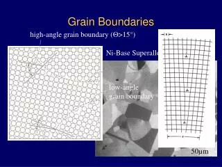
Grain boundaries in ceramics. Grain boundaries Grain boundary: interface between two crystals (grains) of the same phase but different orientation. Regions with: - lower density - different coordination of atoms/ions - relaxation of atomic positions

E N D
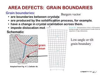
Grain boundaries Grain boundary: interface between two crystals (grains) of the same phase but different orientation. Regions with: - lower density - different coordination of atoms/ions - relaxation of atomic positions - often different composition (segregation of impurities, dopants, lattice defects) - different properties (charge and mass transport, dielectric, optical, etc.) Small angle tilt boundary: misfit accommodated by formation of dislocations Low energy tilt boundary: coincidence of lattice positions
Dislocations Line defects originated by the relative shearing of two parts of a crystal (plastic deformation). Non-equilibrium defects, can not be treated by thermodynamics. Edge dislocation Screw dislocation
Left. HRTEM image of the 5.4 [001] (010) symmetrical tilt grain boundary in SrTiO3. Right. Strain field around the dislocation cores evaluated from the HRTEM image. The size of the lozenges reflects the unit cell size in the respective area. Grain boundaries
110 Sr-O O Imaging of oxygen sublattice and grain boundary structure in SrTiO3 by HRTEM Tilt grain boundary of SrTiO3 The intensity profile along the g.b. shows that the intensity of the O column s is variable. Column with oxygen vacancies Simulated image. Half oxygen atoms were removed from one O column on the g.b. (white arrow). The oxygen deficiency produces a higher brightness in this position (). Central dotted lines connect CSL positions (CSL: coincidence site lattice)
Expansion compared to perfect lattice Sr(CSL)-Sr(CSL) Ti-Ti Sr-Sr Decreased spacing Increased spacing Differences of Ti-Ti spacing along the direction perpendicular to the g.b. The spacing closer to the g.b. is smaller. Increased separation of the two Ti columns facing each other at the g.b. Differences of Sr-Sr spacing along the direction perpendicular to the g.b. The spacing closer to the g.b. is larger. Decreased separation of the two Sr columns facing each other at the g.b. Differences normal to the g.b. of Sr-Sr spacings located on CSL sites. The first spacing is increased meaning that there is an expansion of the g.b. (0.043 nm, 1% lattice parameter). Relaxation of atomic positions near the grain boundary Observed displacements and grain boundary expansion in agreement with first-principle calculations (0.06 nm expansion). Expansion related to Ti-Ti repulsion and existence of O vacancies on the g.b.
250 ppm MgO 250 ppm CaO 1000 ppm La2O3 Segregation in alumina ceramics as visualized by SIM Segregation at grain boundaries Surface tension or surface energy Natural tendency to minimize the surface energy of a system by redistribution of the components. Components which lower the surface/interface energy tend to concentrate at the surface/interface (adsorption, segregation). Oxygen is strongly surface-active in liquid metals and non-oxide ceramics. Segregation at surfaces and grain boundaries in ceramics is determined by the different formation energies of defects at interfaces than in bulk.
Basal plane Segregation in alumina ceramics – atomistic simulation Segregation modifies the energy of the different crystallographic surfaces and, consequently, the equilibrium shape of crystals Surface energies of pure and Y-doped -Al2O3 Interfacial energies of pure and Y-doped -Al2O3 Equilibrium morphologies of undoped -alumina (a) front and (b) top view. Equilibrium morphologies of 10 ppm Y-doped -alumina at 1600°C seen again from (c) front and (d) top view. Wulff’s theorem for the equilibrium shape i: surface tension of ith face hi: distance from the center
Segregation in alumina ceramics – atomistic simulation Predicted grain boundary structures For highly symmetric (left) and more general case (right). Calculated grain boundary structure showing a regular La pattern resulting from segregation.
Segregation in alumina ceramics – atomistic simulation Enthalpy of segregation for La in alumina Calculated and experimental solubility limit of MgO in alumina as a function of grain size
LV SV SL θ > 90°: nonwetting < 90°: wetting = 0°: spreading Grain boundary phases and films In many cases, solid phases located at grain boundaries result from the solidification of a liquid phase formed during sintering. The grain boundary phase can form a continuous film, pockets at the triple junctions or discrete particles. Wetting of a liquid on a solid Necessary condition for spreading: Wetting of grain boundaries Liquid phase forming additives in ceramic oxides: SiO2, glass, alkaline oxides (Li2O, Na2O, K2O), alkaline-earth oxides (CaO, SrO, BaO), TiO2, B2O3, CuO, ZnO, V2O5
CaO:Si3N4 Y2O3:ZrO2 (1) (2) (3) AlN (2) (4) Si3N4 (3) (4) Y2O3:ZrO2 AlN Distribution of liquid/amorphous phase at grain boundaries (1)
No grain boundary layer A A Distribution of liquid/amorphous phase at grain boundaries “Special” grain boundaries show little segregation and are free of an amorphous grain boundary layer Criterion for film formation: GBC Grain boundaries in SrTiO3 ceramics Special (A) + random (B) grain boundaries (rotation) 2A: interfacial energy of a gb containing a wetting amorphous phase GBC: interfacial energy of a clean gb Random grain boundary
Distribution of secondary phase at grain boundaries Ordered grain boundary phase in Ti-rich BaTiO3 ceramics
Segregation and space charge at grain boundaries The defect formation energies and defect chemistry at the grain boundaries is, in general, different from that of the bulk. Preferential segregation of charged defects in ionic solids leads to net charge at the grain boundary core which is compensated by a space charge cloud of opposite sign adjacent to the boundary, with formation of an electrostatic Schottky barrier. The thickness of the space charge layer is of the order of the Debye length. r: relative dielectric constant z: number of charges on defect c: defect concentration in the bulk Schematic diagram of a positively charged grain boundary (segregation of oxygen vacancies) and compensating space charge (acceptor impurity). The region adjacent to the grain boundary will be depleted in oxygen vacancies. L is the width of the space-charge layer L = 2.5 nm in Y-doped ZrO2.
Segregation and space charge at grain boundaries Transport through a polycrystal. Due to anisotropy of grain boundaries and their specific topology, different situations are encountered: (a) parallel effects, (b) perpendicular effects and (c) e flux constriction.
The effect of grain boundaries on the properties of ceramic oxides
[VO••] [VO••] [VO••] [VO••]∞ [VO••]∞ [VO••]∞ + + + + + + + + + + + + + + + + + + D D D 2 Dopant segregation: decreasing effective bulk dopant concentration Space charge effect Because of the high density of gbs in nanoceramics, the total conductivity (not shown) is dominated by the resistive grain boundaries. Ionic conductivity in oxides: the effect of grain boundaries and grain size Oxygen conduction in Y-doped ZrO2 The segregation of oxygen vacancies in acceptor-doped oxygen conducting electrolytes (Y:ZrO2, Gd:CeO2. Fe:SrTiO3) leads to positively charged grain boundaries cores and a depletion of oxygen vacancies in the adjacent space charge layer. The combined effect of the electrostatic potential barrier (Schottky barrier) and the depletion layer determines a decrease of the oxygen conductivity at gbs (blocking gbs). In doped zirconia ceramics with clean boundaries the resistivity of gbs is at least two orders of magnitude higher than the bulk resistivity. A size effect is expected for grain dimensions in the nanoscale region (grain size <4λ). Specific bulk and grain boundary conductivity in 3 mol.% Y2O3 doped ZrO2 (oxygen conductor) At present, the minimum grain size (30-40 nm) of dense Y:ZrO2 ceramics is still >> 4λ and strong size effects on ionic conductivity are not observed.
σT versus 1/T Variation of ionic conductivity with the density of interfaces, N/L. d Nanosize effect. Loss of individuality of the single compounds. 16nm d < 8λ 20nm 430nm d=50nm d d > 8λ interface effect Mesoscopic fast ion conduction in thin-film heterostructures Parallel ionic conductivity in CaF2-BaF2 thin-film heterostructures with overall thickness L comprising of N layers of thickness d. The overall thickness (L) is approximately the same in all cases. d = L/N Black lines: reference single phase films; Green lines: semi-infinite space-charge zones (period >8) Red lines: overlapping space-charge regions (period <8)
Time domain Frequency domain Fourier transform v: voltage i: current : angular frequency θ: phase difference Z: impedance C: capacitance j = V(ω) = I(ω) Z(ω) Z(ω) = 1/(C ω j) v(t) = v0sin(ωt) v(t) V(ω) i(t) I(ω) i(t) = i0sin(ωt+θ) V(ω), I(ω) and Z(ω) are complex quantities S Y axis d ω R1 C1 = 1 ω Simple RC circuit R1 ωp R1 C1 = 1 R0+R1 R0 Ionic conductivity in oxides: the effect of grain boundaries and grain size Impedance spectroscopy Solid materials can be described by one (homogeneous single crystal) or more (ceramics, composites) semicircle in the impedance plot. Each semicircle is described by one resistive and one capacitive component.
Sintered 1250°C/2h; gs: 0.38 μm Sintered 1500°C/48h; gs: 5 μm Intrinsic conductivity grain interior grain boundary Total conductivity Ionic conductivity in oxides: the effect of grain boundaries and grain size Proton conduction in Y-doped BaCeO3 Trivial size effect. The lower conductivity (left) of the fine grained ceramic is only due to the higher density of resistive grain boundaries. The specific conductivities (right) are the same irrespective of grain size.
Continuous grain boundary phase Impedance spectra (a) freq. (a) ZrO2: 3 mol % Y2O3 Lenticular grain boundary phase + clean boundaries (b) (b) Bulk resistivity ZrO2: 6 mol % Y2O3 Grain boundary resistivity Ionic conductivity in oxides: the effect of the grain boundary phase
TiO6 octahedra S Ca l Cu Ceramic 102 Hz Relative dielectric constant 106 Hz tanδ Dielectric loss Dissipation factor Colossal permittivity in CaCu3Ti4O12 : the role of interfaces • Perovskite-like, non polar structure • Not a ferroelectric relaxor • Ab-initio calculations: r = 40 • Processing-dependent properties Step-likebehaviour of dielectric constant observed in ceramics as well as in single crystals. Strong frequency dispersion The dielectric constant (real part of dielectric permittivity) is calculated from the measured capacitance C taking into account the sample geometry:
Single crystal 20 Hz Relative dielectric constant 106 Hz Colossal permittivity in CaCu3Ti4O12 : the role of interfaces
} - semiconductive grain interiors; - more insulating grain boundaries and related interfacial polarization - insulating layer at the electrode-ceramic interface; - insulating surface skin IBLC effect – only for ceramics Maxwell-Wagner relaxation semiconducting ceramic } insulating layer also exist in single crystals electrode Brick layer model of a ceramic Colossal permittivity in CaCu3Ti4O12 : the role of interfaces Apparent colossal dielectric constant is of extrinsic oringin and is associated to the electrical heterogeneity of the samples and the contribution of different interfaces: Insulating gbs Semiconducting grains Insulating skin Semiconductingcore
S D d ρgb >> ρb; gb = b Cbdepends only on composition Cgbdepends on microstructure Cgb>>Cb Intrinsic behaviour Colossal permittivity in CaCu3Ti4O12 : the role of interfaces The step-like behaviour of the dielectric constant and all other electrical properties can be reproduced by using equivalent circuit models. l
Strongly nonlinear current-voltage properties Insulting grain boundaries (brown) Topograpic image Current image Fracture surface conducting tip V ceramic electrode Colossal permittivity in CaCu3Ti4O12 : the role of interfaces Inhomogeneous conduction probed by atomic force microscopy (AFM)
εi ≡ Ki’ grain ε1 >> ε2 ε2 εeff ε1 grain boundary d1 ε2 ε1 d2 “clean” boundary Influence of grain size on the dielectric constant of ferroelectric BaTiO3 ceramics Progressive depression of the dielectric constant with decreasing grain size when d1< 1 micron The microstructure of BaTiO3 ceramics corresponds to ferroelectric grains with high dielectric constant (ε1 = 3000-5000) separated by non ferroelectric (ε2 100) grain boundaries (“dead layer”). The NFE gbs do not necessarily imply a second phase grain boundary layer. d2 = 1-3 nm depending on ceramic preparation method.
Domain size and mobility effect Dead layer effect Influence of grain size on the dielectric constant of ferroelectric BaTiO3 ceramics Relative dielectric constant (298 K, 10 KHz) of dense BaTiO3 ceramics, 1998-2006 HPS: hot pressing IP: pseudo isostatic pressing in a multi-anvil cell CSM:combined sintering method SPS: spark plasma sintering 2SS: two-step sintering Dispersion of experimental values related to processing (purity and stoichiometry of powders, sintering method) and microstructure (porosity, second phase grain boundary layer)