Download
1 / 26
260 likes | 465 Views
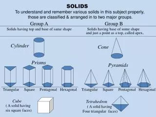
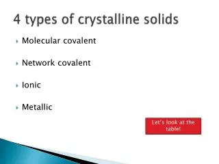
Solids - types. MOLECULAR. Set of single atoms or molecules bound to adjacent due to weak electric force between neutral objects (van der Waals). Strength depends on electric dipole moment No free electrons poor conductors easily deformed, low freezing temperature

E N D
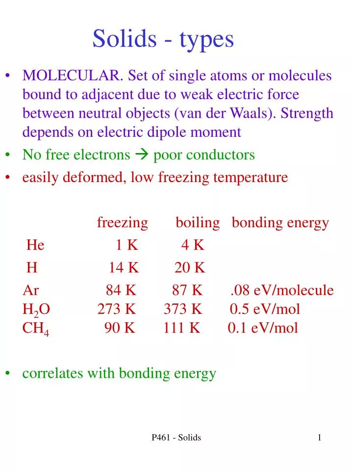
Solids - types • MOLECULAR. Set of single atoms or molecules bound to adjacent due to weak electric force between neutral objects (van der Waals). Strength depends on electric dipole moment • No free electrons poor conductors • easily deformed, low freezing temperature • freezing boiling bonding energy • He 1 K 4 K • H 14 K 20 K • Ar 84 K 87 K .08 eV/molecule H2O 273 K 373 K 0.5 eV/mol CH4 90 K 111 K 0.1 eV/mol • correlates with bonding energy P461 - Solids
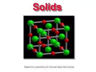
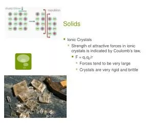
Ionic Solids R Potential vs sep distance R • Positive and negative ions. Strong bond and high melting point. no free electrons poor conductor • similar potential as molecule. ~5 eV molecules and ~6 eV solid (NaCl) • each Cl- has 6 adjacent Na+, 12 “next” Cl-, etc • energy levels similar to molecules except no rotations….electronic in UV and vibrational in IR. Often transparent in visible P461 - Solids
COVALENT. Share valence electrons (C, H, etc) • strong bonds (5-10 eV), rigid solids, high melting point • no free electrons insulators • usually absorb in both visible and UV • METALLIC. s-p shell covalent bonds. But d shell electrons “leftover” (smaller value of n lower energy but larger <r>) • can also be metallic even if no d shell if there is an unfilled band • 1-3 eV bonds, so weaker, more ductile, medium melting temp • “free” electrons not associated with a specific nuclei. Wavelength large enough so wavefunctions overlap and obey Fermi-Dirac statistics conductors EM field of photon interacts with free electrons and so absorb photons at all l P461 - Solids
Bands in Diatomic Molecules-Reminder • assume all valence electrons are shared • if both atoms are the same then |y|2 same if switch atom(1) and atom(2) --- electron densities around each atom are the same (even sort of holds if different atoms like CO) • H(1s) <-- very far apart ---> H(1s) • close together H(“1s”)H(“1s”) • electron wavefunctions overlap -“shared” • two energy levels (S=0,1) (spatial symmetric and antisymmetric)which have E bands R=infinity (atoms) 1s*1s Vib and rot P461 - Solids
Bands in Solids • lowest energy levels very similar to free atoms • large kinetic energy large p, small l • little overlap with electrons in other atoms and so narrow energy band • higher energy levels: larger l wavefunctions of electrons from different atoms overlap • need to use Fermi-Dirac statistics • many different closely spaced levels: Band 4s,4p,3d 3s,3p 2s,2p 1s E P461 - Solids
Multielectron energy levels • 3/2 symmetric spin. Each 1/2 has different mixed symmetry 3 different spacial wavefunctions and (usually) 3 different energy levels • the need for totally antisymmetric wave functions causes the energies to split when the separation distance R < wavelength • if far apart N degenerate(equal) states • overlap still N states but different energy 6 electrons E R P461 - Solids
N different combinations of spatial wavefunctions gives N energy levels • N based on how many electrons overlap large for the outer shell • small DE between different levels an almost continuous energy band • nature of the energy bands determines properties of solid -- filled bands -- empty bands -- partially filled bands -- energy “width” of band -- energy gaps between bands -- density of states in bands P461 - Solids
Bands in Solids 2 • as their atomic radii are larger (and wavelength larger) there is more overlap for outer electrons • larger N (# shared) wider bands (we’ll see later when discuss Fermi gas) • valence electrons will also share though band width is narrower • “valence” vs “conduction” depends on whether band if filled or not conduction valence E P461 - Solids
Conduction vs valence • energy levels in 4s/4p/3d bands overlap and will have conduction as long as there isn’t a large DE to available energy states (and so can readily change states) 00000000 x00000x0 • xxxxxxxx T=0 xxx0xx0x T>0 xxxxxxxx xxxxxxxx xxxxxxxx xxxxxxxx • x=electron 0=empty state (“hole”) • sometime current is due to holes and not electrons • good conductors have 1 or more conduction/free electrons/holes per atom conduction valence E P461 - Solids
Li and Be Bands • Atoms: Li Z=3 1s22s1 unfilled “conductor” Be Z=4 1s22s2 filled “insulator” • But solids have energy bands which can overlap • there is then just a single 2p2s band • Be fills the band more than Li but the “top” (the Fermi Energy) is still in the middle of the band. So unfilled band and both are metals 2p 2s 1s E Atom solid P461 - Solids
Magnesium Bands 6N 3p 3s 8N • Atoms: Z=12 1s22s22p63s2 filled “insulator” like Be • the 3p level becomes a band with 6N energies. The 3s becomes a band with 2N energies • They overlap becoming 1 band with 8N energy levels and no gaps • BUT, if R becomes smaller, the bands split (bonds) giving an energy gap for C, Si, Ge E 2N Atomic separation R P461 - Solids
C,Si,Ge Bands 4N 6N 2p,3p,4p 2s,3s4s • similar valence C:2s22p2Si:3s23p2 Ge:4s24p2 • 8N overlapping energy levels for larger R • R becomes smaller, the bands split into 4N “bond” and 4N “antibond. an energy gap for C (7eV) and Si, Ge (~1 eV) E 4N 2N Atomic separation R empty T=0 E(gap) filled T=0 P461 - Solids
Properties of Energy Bands • Band width, gaps, density of states depend on the properties of the lattice (spacing, structure) • First approximation is Fermi Gas. But if wavelength becomes too small, not overlapping sets width of band • next approximation adds in periodic structure of potential • can cause interference of “traveling” waves (reflection/transmission). Essentially vibrational modes of the solid • destructive interference causes energy gaps which are related to dimensions of lattice • Note often the “band energy” is measured from the bottom of the band (which is the electronic energy level) • “real” calculation needs to use 3D structure of solid complicated D(E), need measurements P461 - Solids
Fermi Gas Model • Quantum Stats: • Ex 13-2. What are the number of conduction electrons excited to E > EF for given T?(done earlier) T=0 T>0 n*D EF P461 - Solids
Fermi Gas Model II ideal real D • Solids have energy bands and gaps • Can calculate density of states D(E) from lattice using Fourier Transform like techniques (going from position to wavelength space) • can change D(E) by changing lattice - adding additional atoms during fabrication - pressure/temperature changes PHYS 566, 480, 690A techniques E P461 - Solids
Fermi Gas Model III Na=L • 1D model. N levels and min/max energy • For 2D/3D look at density of states. Grows as E.5 until circle in k-space “fills up” then density falls (can’t have wavelength ~ smaller than spacing) a ky 2D/3D D kx EF E P461 - Solids
Interactions with Lattice • Study electron wavefunction interactions with the lattice by assuming a model for the potential • Kronig-Penney has semi-square well and barrier penetration • will sort of look at 1D really 3D and dependent on type of crystal which gives inter-atom separation which can vary in different directions • solve assuming periodic solutions • Bragg conditions give destructive interference but different “sine” or “cosine” due to actual potential variation.will have different points where wavefunction=0 V0 P461 - Solids
Interactions with Lattice • Get destructive interference at • leads to gaps near those wavenumbers • once have energy bands, can relate to conductivity • materials science often uses the concept of effective mass. Electron mass not changing but “inertia” (ability to be accelerated/move) is. So high m* like being in viscous fluid larger m* means larger interaction with lattice, poor conductor • m* ~ m in middle of unfilled band m* > m near top of almost filled band m* < m near bottom of unfilled band • always dealing with highest energyelectron (usually near Fermi energy) P461 - Solids
Semiconductors • Filled valence band but small gap (~1 eV) to an empty (at T=0) conduction band • look at density of states D and distribution function n • Fermi energy on center of gap for undoped. Always where n(E)=0.5 (problem 13-26) • D(E) typically goes as sqrt(E) at top of valence band and at bottom of conduction band n D conduction valence EF D*n If T>0 P461 - Solids
Semiconductors II • Distribution function is • so probability factor depends on gap energy • estimate #electrons in conduction band of semiconductor. Integrate over n*D factors at bottom of conduction band P461 - Solids
Number in conduction band using Fermi Gas model = • integrate over the bottom of the conduction band • the number in the valence band is about • the fraction in the conduction band is then P461 - Solids
Conduction in semiconductors • INTRINSIC. Thermally excited electrons move from valence band to conduction band. Grows with T. • “PHOTOELECTRIC”. If photon or charged particle interacts with electrons in valence band. Causes them to acquire energy and move to conduction band. Current proportional to number of interactions (solar cells, digital cameras, particle detection….) • EXTRINSIC. Dope the material replacing some of the basic atoms (Si, Ge) in the lattice with ones of similar size but a different number (+- 1) of valence electrons P461 - Solids
Doped semiconductors • Si(14) 3s23p2 P(15) 3s23p3Al(13) 3s23p1 Si || 4 covalent bonds. Fill all valence Si= Si =Si energy levels (use all electrons) || 1 eV gap Si Si || single electron loosely bound to P Si= P =Si (~looks like Na) || 0.05 eV conduction band Si Si =Si || || 0.06 eV can break one of the Si=Si Si= Al -Si bonds. That electron Al. The “hole” || || || moves to the Si atom Si=Si e “hole” P461 - Solids
Doped semiconductors II conduction band .05 eV donor electrons acceptor holes E .06 eV • The Fermi Energy is still where n(EF) = ½. doping moves EF • Complex compounds shift Fermi Energy and D(E) (AlxOyYz...) valence band P-doped n-type “extra” e .05 eV to move from donor to conduction band Al-doped p-type “missin” e= (hole) .06 eV to move from valence to conduction band P461 - Solids
Doped Semiconductors III • Adding P (n-type). Since only .05 eV gap some electrons will be raised to conduction band where n(E)= ½ is in donor band • adding Al (p-type). some electrons move from valence to acceptor band. n(E)= ½ now in that band n-type D conduction valence EF D(E) p-type EF P461 - Solids
Doped Semiconductors IV • undoped semicon. have Ncond ~ 10-11Nvalence • doping typically 10-7 increases conductivity • but if raise T then the probability to move from valence band to conduction band increases e-E/kT. Can see this as a change in Fermi Energy with temperature at some point all the donor electrons are in the conduction band and many valence move to conduction EF back in middle of gap donor E EF T P461 - Solids