Download
1 / 7
70 likes | 212 Views
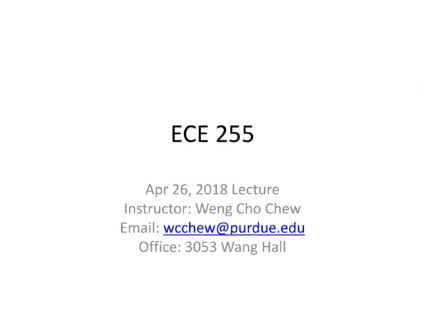
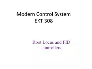
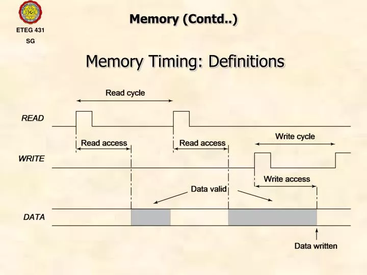
ETEG 431 SG. Memory (Contd..). Memory Timing: Definitions. Non-Volatile Read-Write Memory. Read-Write Memory. Read-Only Memory. Random. Non-Random. EPROM. Mask-Programmed. Access. Access. 2. E. PROM. Programmable (PROM). FLASH. FIFO. SRAM. LIFO. DRAM. Shift Register. CAM.

E N D
ETEG 431 SG Memory (Contd..) Memory Timing: Definitions
Non-Volatile Read-WriteMemory Read-Write Memory Read-Only Memory Random Non-Random EPROM Mask-Programmed Access Access 2 E PROM Programmable (PROM) FLASH FIFO SRAM LIFO DRAM Shift Register CAM ETEG 431 SG Memory Semiconductor Memory Classification
BL BL BL VDD WL WL WL 1 BL BL BL WL WL WL 0 GND Diode ROM MOS ROM 1 MOS ROM 2 ETEG 431 SG Memory Read-Only Memory Cells
BL [0] BL [1] BL [2] BL [3] WL [0] V DD WL [1] WL [2] V DD WL [3] V bias Pull-down loads ETEG 431 SG Memory MOS OR ROM
20 V 0 V 5 V 20 V 0 V 5 V S D S D S D Avalanche injection Removing programming voltage leaves charge trapped Programming results in higher V . T ETEG 431 SG Memory EPROM: Floating-Gate Transistor Programming
Gate Floating gate Drain Source 20 – 30 nm 1 1 n n Substrate p V 10 nm DD ETEG 431 SG Memory WL EEPROM
Control gate Floating gate erasure Thin tunneling oxide 1 1 n source n drain programming p- substrate ETEG 431 SG Memory Flash EEPROM