Download
1 / 34
340 likes | 575 Views
Monolithic Electronics for Multi-channel Detectors. Paul O’Connor, Brookhaven National Laboratory Workshop on position-sensitive Neutron Detectors, June 28 – 30, 2001. Outline. Monolithic circuits for scientific research Technology selection and access

E N D
Monolithic Electronics for Multi-channel Detectors Paul O’Connor, Brookhaven National Laboratory Workshop on position-sensitive Neutron Detectors, June 28 – 30, 2001
Outline • Monolithic circuits for scientific research • Technology selection and access • Preamplifier and shaping amplifier design • Impact of scaling • BNL preamp/shaper examples • Sampling systems • Peak detection and derandomization • Summary and future directions
Monolithic Front Ends • Can be efficiently mass-produced with excellent economy of scale: • E.g., maskset + 10 wafers ~ $100K, 500 chips/wafer • Additional wafer ~ $5K • Incremental cost ~ $10/chip • Chip may have 16 – 128 channels • Can be located close to dense detector electrode arrays • pixels, micropattern & segmented cathode designs • Can combine functions on single chip, replacing PCB/hybrid/cable connections with lower cost on-chip connection • Can reduce power*
Cost of Interconnect ISSCC 2000
Bipolar Workhorse of “old” analog Available from a handful of vendors Speed/power advantage over CMOS (diminishing) Low integration density Standard CMOS Suitable for most analog designs Best for combining analog and digital Highest integration density Widely available Short life cycle (3 years/generation) BiCMOS Complex process, viability uncertain Silicon on insulator (SOI) Modest speed advantage for digital Drawbacks for analog SiGe Complexity equivalent to BiCMOS Extremely fast bipolar device plus submicorn CMOS Availability increasing GaAs Unsuitable for wideband analog Custom Monolithics – technology options
Access to Monolithic Processes Multiproject (shared wafer) foundry runs In the U.S. MOSIS service www.mosis.org Europe Europractice www.imec.be/europractice Design tools Public domain MAGIC bach.ece.jhu.edu/~tim/programs/magic/magic7.html vlsi.cornell.edu/magic Commercial Cadence www.cadence.com Mentor www.mentor.com Tanner www.tanner.com
Preamplifier Design: Front Transistor Optimization • For MOSFETs, the input device must be properly dimensioned to match Cdet: • 1/f noise minimized for Cgs = Cdet • Series thermal noise minimized for Cgs < Cdet, exact value depends on Cdet/Id • For Bipolar transistors, must choose the collector current • Depends on Cdet/tm • MOS will have superior noise when • tm/tel > bBJT • kT/KF > bBJT • Bipolarfavored for short shaping, low power.
all charge preamplifiers need DC feedback element to discharge CF usually, a resistor in the MW – GW range is used monolithic processes don’t have high value resistors we need a circuit that behaves like a high resistor and is also insensitive to process, temperature, and supply variation low capacitance lowest possible noise linear Preamp Reset – Requirements
Preamp Reset –Configurations
Classical RF ∙ CF = RC ∙CC Zero created by RC,CC cancels pole formed by RF, CF IC Version CC = N ∙ CF (W/L)MC = N ∙ (W/L)MF Zero created by MC, CC cancels pole formed by MF, CF Rely on good matching characteristics of CMOS FETs and capacitors Nonlinear Pole-zero Compensation G. Gramegna, P. O’Connor, P. Rehak, S. Hart, “CMOS preamplifier for low-capacitance detectors”, NIM-A 390, May 1997, 241 – 250.
Follow-the-leader Pulse Shaping with Monolithic Circuits • Passive components in monolithic technology are non-ideal: • Tolerance typically ±20% from lot to lot. • Values restricted to C < 50 pF, R < 100K. • Difficulty in setting accurate filter time constants • Low supply voltage in submicron CMOS (1.8 – 3.3V) • Restricts dynamic range • Feedback circuits give the most stable and precise shaping • But require more power than other approaches Filter topologies
8008 4004 CMOS Scaling DRAM • Driven by digital VLSI circuit needs • Goals: in each generation • 2X increase in density • 1.5X increase in speed • Control short channel effects • Maintain reliability level of < 1 failure in 107 chip-hours Intel microprocessor
Year 85 88 91 94 97 00 02 04 07 10 13 Min. feature size [mm] 2 1.5 1.0 0.7 0.5 0.35 0.25 0.18 0.13 0.10 0.07 Gate oxide [nm] 44 33 22 16 11 7.7 5.5 4.0 2.9 2.2 1.6 Power supply [V] 5 5 5 5 5/3.3 3.3 2.5 1.8 1.2 1 .7 Threshold voltage [V] 1.0 0.9 0.8 0.7 0.6 0.5 0.45 0.4 0.3 0.3 0.3 CMOS Technology Roadmap
CMOS scaling and charge amplifier performance • Fundamental noise mechanisms • so far, no dramatic changes with scaling • Noise • slight improvement with scaling • higher device fT reduces series thermal noise • Weak- and moderate inversion operation more common • need different matching to detector capacitance. • Reduced supply voltage • difficult to get high dynamic range • Many difficulties with “end of the roadmap” devices P. O’Connor, G. DeGeronimo, “Charge amplifiers in scaled CMOS”, NIM-A accepted for publication
Impact of technology scaling on charge amplifier performance 4 detector scenarios for scaling study Noise vs. scaling (power held constant) Power vs. scaling (noise held constant)
Used with ultra-low capacitance silicon drift detector, Cdet < 0.3 pF Preamp only, used with external shaper Purpose: explore lowest noise possible with CMOS Reset system: MOS transistor with special bias circuit to achieve stable, > 100 GW equivalent resistance Detector Drift Detector Preamplifier
Spectra of 241Am and 55Fe taken with 5mm F Si drift detector and CMOS X-ray preamplifier. Detector and circuit cooled to -75 C. External 2.4 ms shaping. ENC = 13 e- rms. Noise without detector: 9 e- Drift detector preamplifier – results P. O'Connor et.al., "Ultra Low Noise CMOS Preamplifier-shaper for X-ray Spectroscopy", NIM A409 (1998), 315-321
Time Expansion Chamber & Transition Radiation Detector Preamp/Shaper • 1m MWPC with 20 pF CDET • Fast (70 ns) shaping for charged particle tracking • Dual gain outputs for measurement of dE/dx and Transition Radiation
TEC-TRD Preamp/Shaper Block Diagram Die Layout X-ray Response A. Kandasamy, E. O’Brien, P. O’Connor, W. VonAchen, “A monolithic preamplifier-shaper for measurement of energy loss and transition radiation” IEEE Trans. Nucl. Sci. 46(3), June 1999, 150-155
Direct connection to low-capacitance (3 pF) silicon drift detector Fast shaping (50 ns) for tracking Low power requirement (< 5 mW/chan.) Silicon bipolar technology Silicon Vertex Tracker Preamp/Shaper
SVT Preamp/Shaper Die Layout Output Waveform
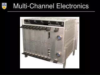
SVT 240-channel Multi-Chip Module D. Lynn et al., “A 240 channel thick film multi-chip module for readout of silicon drift detectors”, NIM A439 (2000), 418 - 426
Practical amplifier considerations • Preamplifier reset • High order filters • Programmable pulse parameters • Circuit robustness: • Self-biasing • Low-swing,differential I/O • Circuits tolerant to variations in • Temperature • Process • Power supply • DC leakage current • Loading Peaking time variation G. De Geronimo et.al., “A generation of CMOS readout ASICs for CZT detectors", IEEE Trans. Nucl. Sci. 47, Dec. 2000, 1857 - 1867
What goes between the preamp/shaper and the ADC? • Experimental needs differ • number of channels • occupancy • rate • trigger • Usually, its too expensive to put an ADC per channel • Anyway the ADC would usually not be doing anything useful • Occupancy < 100%, so no events most of the time in most channels • What is the most efficient way to use the ADC(s)?
Analog Sampling and Multiplexing Track-and-hold (triggered systems) Analog memory (non-triggered)
New Peak Detector and Derandomizer • Self-triggered • Self-sparsifying • New 2-phase configuration allows rail-to-rail operation, eliminates offsets • absolute accuracy ~ 0.2% • to within 300 mV of rails • Two or more peak detectors in parallel can be used to derandomize events • If a second pulse arrives before the readout of the first pulse in Pd-a, it is detected and stored on Pd-b.
0.2% First experimental results Accuracy of single PD PD/D response to random pulse train (241Am on CZT) G. DeGeronimo, P. O’Connor, A. Kandasamy, “Analog Peak Detect and Hold Circuits Part 2: The Two-Phase Offset-Free and Derandomizing Configurations”, NIM-A submitted for publication
Summary and Future Directions • Today’s monolithic technology can be used effectively for low-noise front ends. • Technology scaling, by reducing the area and power per function, wil allow increasingly sophisticated signal processing on a single die. • Integrated sensors will be developed for some X-ray and charged-particle tracking applications. • Interconnecting the front end to the detector and to the rest of the system will continue to pose challenges.