Download
1 / 1
10 likes | 127 Views
Toxicity Assay-on-Chip for Engineered Nanomaterials Komal Garde, Steven Crawford and Shyam Aravamudhan* Department of Nanoengineering, Joint School of Nanoscience and Nanoengineering North Carolina A&T State University, Greensboro, NC *Tel: 9336) 285-285-2856, Email: saravamu@ncat.edu.

E N D
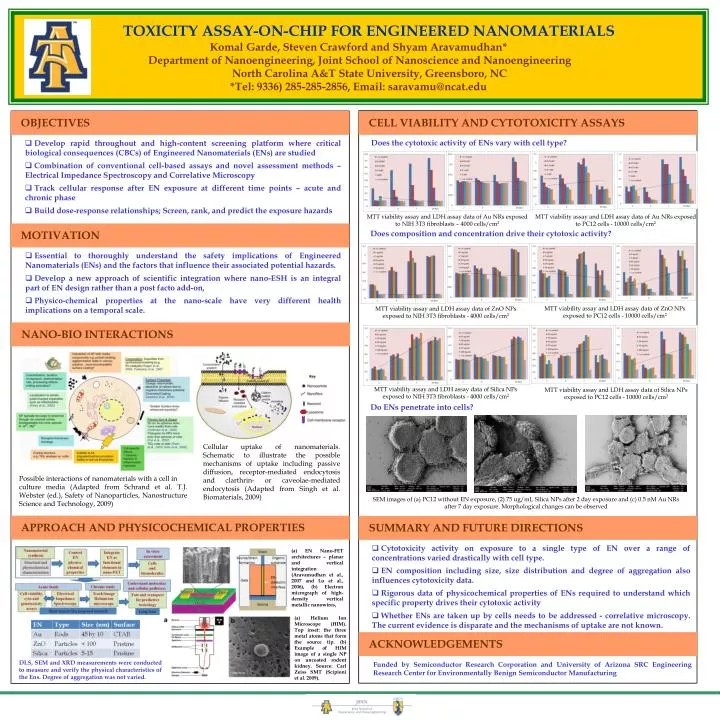
Toxicity Assay-on-Chip for Engineered NanomaterialsKomal Garde, Steven Crawford and Shyam Aravamudhan* Department of Nanoengineering, Joint School of Nanoscience and Nanoengineering North Carolina A&T State University, Greensboro, NC*Tel: 9336) 285-285-2856, Email: saravamu@ncat.edu Objectives Cell viability and cytotoxicity assays • Develop rapid throughout and high-content screening platform where critical biological consequences (CBCs) of Engineered Nanomaterials (ENs) are studied • Combination of conventional cell-based assays and novel assessment methods – Electrical Impedance Spectroscopy and Correlative Microscopy • Track cellular response after EN exposure at different time points – acute and chronic phase • Build dose-response relationships; Screen, rank, and predict the exposure hazards Does the cytotoxic activity of ENs vary with cell type? MTT viability assay and LDH assay data of Au NRs exposed to NIH 3T3 fibroblasts – 4000 cells/cm2 MTT viability assay and LDH assay data of Au NRs exposed to PC12 cells - 10000 cells/cm2 Motivation Does composition and concentration drive their cytotoxic activity? • Essential to thoroughly understand the safety implications of Engineered Nanomaterials (ENs) and the factors that influence their associated potential hazards. • Develop a new approach of scientific integration where nano-ESH is an integral part of EN design rather than a post facto add-on, • Physico-chemical properties at the nano-scale have very different health implications on a temporal scale. MTT viability assay and LDH assay data of ZnO NPs exposed to PC12 cells - 10000 cells/cm2 MTT viability assay and LDH assay data of ZnO NPs exposed to NIH 3T3 fibroblasts - 4000 cells/cm2 Nano-Bio Interactions MTT viability assay and LDH assay data of Silica NPs exposed to NIH 3T3 fibroblasts - 4000 cells/cm2 MTT viability assay and LDH assay data of Silica NPs exposed to PC12 cells - 10000 cells/cm2 Do ENs penetrate into cells? Cellular uptake of nanomaterials. Schematic to illustrate the possible mechanisms of uptake including passive diffusion, receptor-mediated endocytosis and clarthrin- or caveolae-mediated endocytosis (Adapted from Singh et al. Biomaterials, 2009) Possible interactions of nanomaterials with a cell in culture media (Adapted from Schrand et al. T.J. Webster (ed.), Safety of Nanoparticles, Nanostructure Science and Technology, 2009) SEM images of (a) PC12 without EN exposure, (2) 75 ug/mL Silica NPs after 2 day exposure and (c) 0.5 nM Au NRs after 7 day exposure. Morphological changes can be observed Approach and Physicochemical properties Summary and future directions • Cytotoxicity activity on exposure to a single type of EN over a range of concentrations varied drastically with cell type. • EN composition including size, size distribution and degree of aggregation also influences cytotoxicity data. • Rigorous data of physicochemical properties of ENs required to understand which specific property drives their cytotoxic activity • Whether ENs are taken up by cells needs to be addressed - correlative microscopy. The current evidence is disparate and the mechanisms of uptake are not known. (a) EN Nano-FET architectures – planar and vertical integration (Aravamudhan et al., 2007 and Lu et al., 2006), (b) Electron micrograph of high-density vertical metallic nanowires, (a) Helium Ion Microscope (HIM). Top inset: the three metal atoms that form the source tip. (b) Example of HIM image of a single NP on uncoated rodent kidney. Source: Carl Zeiss SMT (Scipioni et al. 2009). Acknowledgements • Funded by Semiconductor Research Corporation and University of Arizona SRC Engineering Research Center for Environmentally Benign Semiconductor Manufacturing DLS, SEM and XRD measurements were conducted to measure and verify the physical characteristics of the Ens. Degree of aggregation was not varied.