Download
1 / 15
380 likes | 1.41k Views
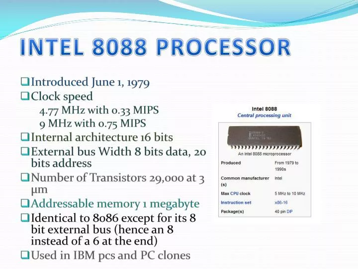
INTEL 8088 PROCESSOR. Introduced June 1, 1979 Clock speed 4.77 MHz with 0.33 MIPS 9 MHz with 0.75 MIPS Internal architecture 16 bits External bus Width 8 bits data, 20 bits address Number of Transistors 29,000 at 3 µm Addressable memory 1 megabyte

E N D
INTEL 8088 PROCESSOR • Introduced June 1, 1979 • Clock speed 4.77 MHz with 0.33 MIPS 9 MHz with 0.75 MIPS • Internal architecture 16 bits • External bus Width 8 bits data, 20 bits address • Number of Transistors 29,000 at 3 µm • Addressable memory 1 megabyte • Identical to 8086 except for its 8 bit external bus (hence an 8 instead of a 6 at the end) • Used in IBM pcs and PC clones
INTEL80186 • Introduced 1982 • Used mostly in embedded applications - controllers, point-of-sale systems, terminals, and the like • Used in several MS-DOS non-PC-Compatible computers including RM Nimbus, Tandy 2000 • Included two timers, a DMA controller, and an controller on the chip in addition to the processor • Later renamed the iAPX 186
OTHER PROCESSORS OF 16 BIT Intel 80188 • VARIOUS OTHER PROCESSORS WHICH EVOLVED WITH SOME DIFFERENCE ARE[WITH 16 BIT] • 80188 • 80286
PROCESSORS OF 32 BITS VARIOUS NAMES Here celeron 2,3 are • Pentium1 • Pentium 2 • Celeron 2 • Pentium 3 • Celeron 3 • Celeron M • Celeron D • The improvement of pentium 1 and 2 respectively
Description of pentium 1 • Bus width 64 bits • System bus speed 60 or 66 MHz • Address bus 32 bits • Addressable Memory 4 GB • Virtual Memory 64 TB • Superscalar architecture brought 5X the performance of the 33 MHz 486DX processor • Runs on 5 volts • Used in desktops • 16 KB of L1 cache
P5 - 0.8 µm process technology • Introduced March 22, 1993 • Number of transistors 3.1 million • Socket 4 273 pin PGA processor package • Package dimensions 2.16" x 2.16" • Family 5 model 1 • Variants • 60 MHz with 100 MIPS (70.4 SPECint92, 55.1 SPECfp92 on Xpress 256 KB L2) • 66 MHz with 112 MIPS (77.9 SPECint92, 63.6 SPECfp92 on Xpress 256 KB L2) • P54 - 0.6 µm process technology • Socket 7296/321 pin PGA package • Number of transistors 3.2 million • Variants • 75 MHz Introduced October 10, 1994 • 90 MHz Introduced March 7, 1994 • 100 MHz Introduced March 7, 1994 • 120 MHz Introduced March 27, 1995 • P54C - 0.35 µm process technology • Number of transistors 3.3 million • 90 mm² die size • Family 5 model 2 • Variants • 120 MHz Introduced March, 1995 • 133 MHz Introduced June, 1995 • 150 MHz Introduced January 4, 1996 • 166 MHz Introduced January 4, 1996 • 200 MHz Introduced June 10, 1996
Celeron [pentium 2 based] Description Structure • Covington - 0.25 µm process technology • Introduced April 15, 1998 • 242-pin Slot 1 SEPP (Single Edge Processor Package) • Number of transistors 7.5 million • 66 MHz system bus speed • Slot 1 • 32 KB L1 cache • No L2 cache • Variants • 266 MHz Introduced April 15, 1998 • 300 MHz Introduced June 9, 1998 • Mendocino - 0.25 µm process technology • Introduced August 24, 1998 • 242-pin Slot 1 SEPP (Single Edge Processor Package), Socket 370 PPGA package • Number of transistors 19 million • 66 MHz system bus speed • Slot 1, Socket 370 • 32 KB L1 cache • 128 KB integrated cache • Family 6 model 6
Pentium 2 • Introduced May 7, 1997 • Pentium Pro with MMX and improved 16-bit performance • 242-pin Slot 1 (SEC) processor package • Slot 1 • Number of transistors 7.5 million • 32 KB L1 cache • 512 KB ½ speed external L2 cache • The only Pentium II that did not have the L2 cache at ½ speed of the core was the Pentium II 450 PE. • Klamath - 0.35 µm process technology (233, 266, 300 MHz) • 66 MHz system bus speed • Family 6 model 3 • Variants • 233 MHz Introduced May 7, 1997 • 266 MHz Introduced May 7, 1997 • 300 MHz Introduced May 7, 1997 • Deschutes - 0.25 µm process technology (333, 350, 400, 450 MHz) • Introduced January 26, 1998 • 66 MHz system bus speed (333 MHz variant), 100 MHz system bus speed for all models after • Family 6 model 5
Pentium 3 and celeron[based on p3] Pentium 3 Celeron • Introduced February 26, 1999 • Improved PII, i.e. P6-based core, now including Streaming SIMD Extensions (SSE) • Number of transistors 9.5 million • 512 KB ½ speed L2 External cache • 242-pin Slot 1 SECC2 (Single Edge Contact cartridge 2) processor package • System Bus Speed 100 MHz, 133 MHz (B-models) • Slot 1 • Family 6 model 7 • Variants • 450 MHz Introduced February 26, 1999 • 500 MHz Introduced February 26, 1999 • 550 MHz Introduced May 17, 1999 • 600 MHz Introduced August 2, 1999 • 533 MHz Introduced (133 MHz bus speed) September 27, 1999 • 600 MHz Introduced (133 MHz bus speed) September 27, 1999 • Coppermine - 0.18 µm process technology • Introduced October 25, 1999 • Number of transistors 28.1 million • 256 KB Advanced Transfer L2 Cache (Integrated) • 242-pin Slot-1 SECC2 (Single Edge Contact cartridge 2) processor package, 370-pin FC-PGA (Flip-chip pin grid array) package • System Bus Speed 100 MHz (E-models), 133 MHz (EB models) • Slot 1, Socket 370 • Family 6 model 8 • Coppermine-128, 0.18 µm process technology • Introduced March, 2000 • Streaming SIMD Extensions (SSE) • Socket 370, FC-PGA processor package • Number of transistors 28.1 million • 66 MHz system bus speed, 100 MHz system bus speed from January 3, 2001 • 32 kB L1 cache • 128 kB Advanced Transfer L2 cache • Family 6 model 8
Pentium 4 Structure of pentium 4 Description of P4 • 0.18 µm process technology (1.40 and 1.50 GHz) • Introduced November 20, 2000 • L2 cache was 256 KB Advanced Transfer Cache (Integrated) • Processor Package Style was PGA423, PGA478 • System Bus Speed 400 MHz • SSE2,SIMD Extensions • Number of Transistors 42 million • Used in desktops and entry-level workstations • 0.18 µm process technology (1.7 GHz) • Introduced April 23, 2001 • See the 1.4 and 1.5 chips for details • 0.18 µm process technology (1.6 and 1.8 GHz) • Introduced July2, 2001 • See 1.4 and 1.5 chips for details • Core Voltage is 1.15 volts in Maximum Performance Mode; 1.05 volts in Battery Optimized Mode • Power <1 watt in Battery Optimized Mode • Used in full-size and then light mobile PCs • 0.18 µm process technology Willamette (1.9 and 2.0 GHz) • Introduced August 27, 2001 • See 1.4 and 1.5 chips for details • Family 15 model 1 • Pentium 4 (2 GHz, 2.20 GHz) • Introduced January 7, 2002 • Pentium 4 (2.4 GHz) • Introduced April 2, 2002
0.13 µm process technology Northwood A (1.7, 1.8, 1.9, 2, 2.2, 2.4, 2.5, 2.6, 2.8(OEM),3.0(OEM) GHz) • Improved branch prediction and other microcodes tweaks • 512 KB integrated L2 cache • Number of transistors 55 million • 400 MHz system bus. • Family 15 model 2 • 0.13 µm process technology Northwood B (2.26, 2.4, 2.53, 2.66, 2.8, 3.06 GHz) • 533 MHz system bus. (3.06 includes Intel's hyper threading technology). • 0.13 µm process technology Northwood C (2.4, 2.6, 2.8, 3.0, 3.2, 3.4 GHz) • 800 MHz system bus (all versions include Hyper Threading) • 6500 to 10000 MIPS
In next slide we will diffrentiate in the working of single and duo core