Download
1 / 13
170 likes | 372 Views
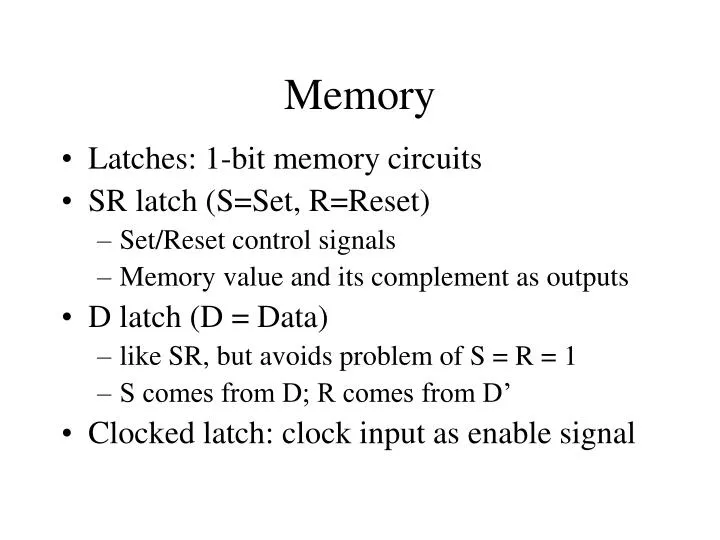
Memory. Latches: 1-bit memory circuits SR latch (S=Set, R=Reset) Set/Reset control signals Memory value and its complement as outputs D latch (D = Data) like SR, but avoids problem of S = R = 1 S comes from D; R comes from D’ Clocked latch: clock input as enable signal. An SR Latch.

E N D
Memory • Latches: 1-bit memory circuits • SR latch (S=Set, R=Reset) • Set/Reset control signals • Memory value and its complement as outputs • D latch (D = Data) • like SR, but avoids problem of S = R = 1 • S comes from D; R comes from D’ • Clocked latch: clock input as enable signal
Flip-Flops • Flip-flops have same function as latches • Flip-flops are edge-triggered • Latches are level-triggered • Flip-flops typically used in industry
Registers • Essentially a group of flip-flops • Common control signals • Different data signals • Distinct from main memory and cache • Typically found at the heart of the CPU
Memory Circuit Notes • Data input lines (typically word size) • Data output lines (also word size) • Address lines • typically less than word size per memory IC • chip select line • Read/write indicator line • Output enable buffers (disconnects bus)
4 Mbit Memory Chip Notes • Multiple chips in a series • Chip select = highest order address bit(s) • 512 x 1024 possible addresses • Each address has 8 bits of data • Control signal for reading/writing (WE) • Control signal for output enable (OE) • Control signals are asserted to indicate “on”
Cache (pp. 77-80, 293-298) • Spatial locality and temporal locality • Split into two areas: data and instructions • Mean access time = c + (1 - h) * m • Where c is cache access time • And h is the hit ratio • And m is main memory access time • Cache lines: fixed-size blocks and tags • Direct-mapped versus set-associative
RAM Chips • SRAM: flip-flops • S = static (i.e. “power’s always on”) • DRAM: capacitors • less circuitry/space/power, but slower • D = dynamic (i.e. “refreshed periodically”) • EDO: two-stage pipeline • FPM: fast page mode (cache nearby words) • SDRAM: S=synchronous with clock • DDR: double data rate (access on rise, fall)