Download
1 / 8
80 likes | 546 Views
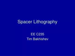
Spacer Lithography Technology. Xin Sun EE235 Presentation Feb 13, 2008. Outline. Introduction Spacer Lithography Process Discussion. IC Technology Advancement. Professor Tsu-Jae King Liu, FLCC Seminar 2006. Lithography Challenges. Continued Scaling of Feature Size Shorter wavelength

E N D
Spacer Lithography Technology Xin Sun EE235 Presentation Feb 13, 2008
Outline • Introduction • Spacer Lithography Process • Discussion
IC Technology Advancement Professor Tsu-Jae King Liu, FLCC Seminar 2006
Lithography Challenges • Continued Scaling of Feature Size • Shorter wavelength • Immersion lithography • Image quality • OPC • Irregularity of masks
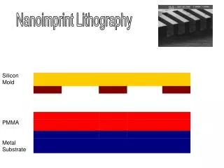
Spacer Lithography Process Yang-Kyu Choi, Ji Zhu, Jeff Grunes, Jeffrey Bokor, and Gabor. A. Somorjai, “Fabrication of Sub-10-nm Silicon Nanowire Arrays by Size Reduction Lithography,” J. Phys. Chem. B 2003, 3340-3343.
Multiplication of Pattern Density 2n lines after n iterations of spacer lithography!
Advantages • Sub-lithographic feature sizes • CVD film thickness determines feature size • Tighter CD control Gate formation by spacer lithography uniform Lg Lg Gate formation by conventional lithography non-uniform Lg Lg Y.-K. Choi et al., IEDM Technical Digest, pp. 259-262, 2002 Y.-K. Choi et al., IEEE Trans. Electron Devices, Vol. 49, p. 436, 2002
Disadvantages • Several spacer lithography steps are needed to obtain different gate lengths. • Additional mask is needed. Geometrical regularity is preferred.