Download
1 / 23
230 likes | 237 Views
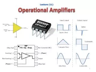
Lecture 7. Operational Amplifiers I. The Op Amp is a voltage – controlled device. The perfect amplifier…almost. Vin = Vdiff → 0 Rin → ∞ Rout → 0 G → ∞. Non-Inverting Amplifier. I in. I in ~ 0 … why? V in ~ V+ ~ V- … why? V diff ~ 0 … why? I out = V out / (R 1 + R 2 ) … why?.

E N D
Lecture 7 Operational Amplifiers I
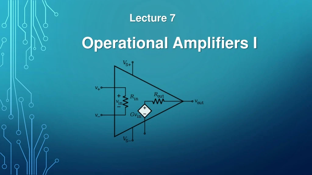
The Op Amp is a voltage – controlled device • The perfect amplifier…almost. • Vin = Vdiff → 0 • Rin → ∞ • Rout → 0 • G → ∞
Non-Inverting Amplifier Iin • Iin ~ 0 … why? • Vin ~ V+ ~ V- … why? • Vdiff ~ 0 … why? • Iout = Vout / (R1 + R2) … why? Vin Iout • Let Vin go positive…V+ input will draw no current! • Vdiff = 0…therefore… • Iout (supplied by op amp) all flows through R1 AND R2 • Vin = V - = V + • Vin = Iout R2 = R2 (Vout / (R1 + R2)) • Gain = G = Vout / Vin = (R1 + R2) / R2 • G = 1 + R1/ R2
The open-loop op amp gain A is infinite…A = ∞. The inputs draw no current…Rin is infinite…Rin = ∞. With negative feedback…the op amp does whatever it can to make Vdiff = 0.
Inverting Amplifier I I • Assume Vin goes positive (the reverse will take place if it goes negative). • Current I flows through R1 and R2 and is “sunk” by the op amp output. • Vdiff = 0 Therefore… • V - = V+ = 0 • I = Vin / R1 • Vout = - I R2 = - Vin (R2 / R1) • G = Vout/ Vin = - R2 / R1
Negative Feedback Vin Vdiff Vout βVout • Vin = V + • Vdiff = V + - V - • Vout = AOLVdiff • V - = βVout • Vdiff = Vin - βVout • Vout= AOL(Vin - βVout) • Vout (1 + β AOL) = Vin AOL • G = Vout / Vin = AOL / (1 + β AOL) ~ 1 / β
How Negative Feedback Affects Zin & R0 Voltage Feedback • A sample βof the output voltage is fed back… • Vin = Vx - βVout… Why? • βVout is the (-) feedback voltage, which reduces the applied input voltage Vx to Vin … (Vin here was called Vdiff previously) • Vx = IxRin + βVout • Vout = AV Vin = AVIxRin … (AV is the open-loop gain) • Vx = IxRin+ β (AV IxRin) • Rin’ = Vx / Ix = Rin (1 + β AV) … (β AV is called the loop gain …) • Rout’ = R0 / (1 + β AV) … ( The output impedance is reduced ) • A sample βof the output current is fed back… • Rin’ = R0 / (1 + β AV) … (The input impedance is reduced ! ) • Rout’ = R0(1 + β AV) … (The output impedance is increased ! )
Non-Inverting Amplifier … again • β = R2 / (R1 + R2) • G = A / (1 + β A) ~ 1 / β • G = (R1 + R2) / R2 • G = 1 + R1/ R2
Inverting Amplifier … again • A more ‘graphic’ way to think…imagine the resistance from input to output is continuous. • What is voltage drop as you ‘move along’ this resistance? (What is V(R) ?) V Vin G = Vout / Vin = - R2 / R1 V = 0 R R1 R2 Vout
Difference Amplifier • Gain of Difference Amplifier • Assume R1 = R2 = R • Ground V2 … apply signal V1 … an inverting amp Vout = - V1 • Ground V1… apply signal V2 … non-inverting amp Vout = V2 • Let V1= V2… Vout = V2 – V1 = 0 • In general then, Vout = V2 – V1 (with all resistors = ). • Formal Derivation… • R1≠ R2 • (i) Vy = V2 [ R2 / ( R1 + R2 ) ] = Vx • (ii) I1 = ( V1 - Vx) / R1= (Vx– Vout ) / R2 • Substitute Vx from (i) into (ii) and with a little algebra… • Vout = (R2 / R1) ( V2 – V1) I1 x y Integrated op amp (INA105A) with uncommitted “sense” and “reference” pins. Resistors matched to +/- 0.01%. Classic dif amp…connect sense to output and ref to gnd. You can make ‘nifty circuits… • Exercise: • Show how to make (i) – (iii) Precision unity gain inverter Non-inverting gain of 2 Non-inverting gain of 0.5 Output to upper sense; in(+) to gnd Output to upper sense; in(-) to gnd Output to upper sense; ref to gnd
Are the Golden Rules Applicable Here? Probably a mistake…the designer wants a really, really high G amplifier…but no feedback and for reasons we’ll soon see, it will move into ‘saturation’. This is a goody…it works fine. It’s called a follower. This is a disaster… it’s feedback is positive…not negative. • The Moral of the Story… • Use feedback • Make sure it’s negative • Keep the op amp in the active region…not saturation.
Are the Golden Rules Applicable Here? (b) (a) • These circuits work…conditionally. • works… but only for (-) inputs…not (+) as shown. Why? • works … but only for (+) inputs…not (-) as shown. Why?
Inverting Amplifier The Follower We get this… Suppose we let R1 → 0 and R2 → ∞ • Extremely useful circuit: • Unity gain buffer • Isolates input and output circuits • High input, low output impedance
More Followers (a) (b) (c) (d) (a) Vout = Vin – VBE Rout = rE Rin = β RE (b) Vout = Vin Rout = 0 Rin = ∞ Iout limited (c) Vout = Vin Rout = 0 Rin = ∞ Iout up to ~ > 1 A But only ‘sources’ Iout (d) Vout = Vin Rout = 0 Rin = ∞ Iout up to ~ > 1 A ‘Sources’ and ‘Sinks’
Class A Audio Amplifier (Note: Goes with BJT lectures) • 10 W loudspeaker amplifier… • Output driven by single-ended emitter follower, Q2 • Dissipates 165 W of quiescent power! … Why? • A single-ended follower operating between split supplies can drive a grounded load up and down ONLY if a high quiescent current is used. • Q1 included for 2 reasons: • (i) reduces drive requirements. • (ii) cancels Q2’s VBE offset, i.e., 0 V in = 0 V out • 100 mA current source provides Q2’s large base current requirement (~ 50 mA) at the top of signal swing. Power Dissipation • Q2 can swing ~ +/- 15 V (9 V rms) • ILOAD ~ (9V / 8Ω~ 1.1 A. PLOAD ~ (9V)(1A) ~ 10 W • With 0V in, P8Ω = (V8Ω)2 / 8Ω= 113 W • IQ2 ~ IE = 30V / 8Ω = 3.75 A, so P8Ω = 3.75A (15V) = 56 W
Push-Pull Output • Q1 sources when signal + • Q2 sinks when signal – • No power dissipation with no signal in. • But…Crossover distortion • Vout lags Vin by VBE • Therefore, Vout ~ 0 between +/- VBE • Biasing remedy • Place push-pull stage into slight conduction. Diodes do that. • As signal “crosses over’ Q1 or Q2 is in conduction. • R must insure enough base current when Q1 or Q2 on hard. • 100 Ω resistor eliminates any “dead zone” during cross over
Cleaning Up Cross-over Distortion • The “SILLY” connection generates a beautiful sinewave at the op amp output, but the output of the push-pull suffers cross-over distortion. • The “SMART” connection uses the magic of feedback to modify the op amp output so that the beautiful sinewave appears at the push-pull output! Class AB Amplifier • Audio speakers have inductance as well as resistance. • The “snubber” circuit is used to prevent ringing.
Cleaning Up Cross-over Distortion SILLY • Scope Traces for resistive load SMART SILLY • Scope Traces for speaker load SMART
Summing Amplifier • Otherwise • Variant of Inverting Amplifier • Point X is a virtual ground • Input is V1 / R1 + V2/ R2 + V3/ R3 • If R1= R2 = R3 = R … Vout = - (V1+ V2+ V3) • Inputs can be + or – • If R’s are unequal…get a weighted sum. • For example…suppose R1 = 2R2 = 4R3 = 8R4 … what do you get?
Transresistance Amplifier I A resistor is a current to voltage converter… otherwise known as a transresistance amplifier. V • Many devices generate currents, eg: • Photodiodes • Phototransistors • Photomultiplier tubes, etc. • Often the currents are small. • They require amplification and conversion into a voltage. • A very large resistor might work, but it might load the output of the current source. B. Phototransistor sources current. Phototransistor used as photodiode to sink current. • Solution… • Use an op amp to source (or sink) the output current through a large resistor. • Careful tho…such circuits are prone to oscillate because of the output capacitance of the source.
Current Sources (a) (b) • Circuit (a) is ~ ideal current source without a transistor’s VBE. ILOAD = Vin / R • Disadvantage I…load “floats” … not tied to ground or a power supply. • eg, Couldn’t generate a sawtooth wave wrt ground. • Disadvantage II…All load current comes from op amp and its output current is almost always limited to small values, say +/- 25 mA. I Vin Vin I • Circuit (b) much better… again… ILOAD = Vin / R but … • (i) Uses transistor to source current, which is provided by power supply. • (ii) Load doesn’t float…it’s tied to power supply. • (iii) Transistor is within feedback loop…op amp feedback eliminates its annoying VBE. • (iv) Op amp eliminates effect of VBE variations with temperature and current. • (v) Op Amp makes transistor a “perfect” current source. Its collector resistance doesn’t matter.
PNP Current Source • Vin = VCC R2 / (R1 + R2) • Iout ~ IE = (VCC – Vin) / R • Iout = VCC (1 - R2 / (R1 + R2)) / R • Iout = VCC(R1 / R) / (R1 + R2) Idiv IE Vin • No VBE offsets • No VBE variations with temperature • No variations of VBE with IC • No variations of VBE with VCE • But IB might vary with VCE, so IC could change even though IE cannot. (IE is stabilized by the op amp…not IC!) • Use a Darlington…or… Use a MOSFET. • Vin is a fixed voltage referenced to VCC… • Suppose you want a variable Vin referenced to gnd! • This circuit does the trick!
Howland Current Source • A “textbook” current source IF R4 / R1 = R3 / R2. • Convert to non-inverting current source by switching Vin and ground. • Resistors must be matched “perfectly”. • Limited by CMRR. • For large currents, R’s must be small; limits compliance. • At hi frequencies, loop gain is low and output impedance can drop from ∞ to 100’s of Ω’s. I1 I4 Vx I2 I3 Solve for (V0 – Vx) Substitute into 2ndeqn above