Download
1 / 14
140 likes | 152 Views
Optical Global Trigger Interface Card. Dual CMC card with Virtex 5 LX110T 16 bidirectional 3.2Gb/s optical links 320 conventional I/O. Introduction. Legacy links from GCT to GT were retained in the revised GCT. Ensured that GCT-GT interface remained the same

E N D
Optical Global Trigger Interface Card Dual CMC card with Virtex 5 LX110T 16 bidirectional 3.2Gb/s optical links320 conventional I/O Trigger Workshop: Greg Iles (g.iles@imperial.ac.uk)
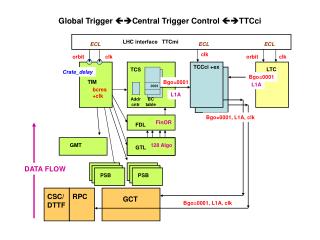
Introduction Legacy links from GCT to GT were retained in the revised GCT. Ensured that GCT-GT interface remained the same Copper high speed links based on National Semiconductor DS92LV16 However, links not robust System in USC55 works, but precarious RCT to GCT Links: Optical links based on 8B/10B GCT to GT Links: Legacy links from old GCT project DC coupled electrical links Trigger Workshop: Greg Iles (g.iles@imperial.ac.uk)
Optical Global Trigger Interface 4x Bidirectional POP4s 3.2 Gb/s at 150m Virtex5-110T > 320 configurable I/O Two I/O bank voltages Use same card for Tx at GCT and Rx at GT Trigger Workshop: Greg Iles (g.iles@imperial.ac.uk)
Optical Global Trigger Interface • Upgraded links to match those between RCT and GCT, albeit based on Xilinx Virtex5-110T • FPGA allows flexibility • Can change link speed/protocol easily • FPGA provides 16 channels at 3.7Gb/s, • Current POP4 fibre optic transceivers limited to 3.2Gb/s • Optical Global Trigger Interface • Running asynchronously at 3Gb/s on all 16 channels • Protected with CRC Check • Automatic link configuration to correct latency • System currently designed to match current requirements • Option to increase bandwidth into GT by factor of >2 Trigger Workshop: Greg Iles (g.iles@imperial.ac.uk)
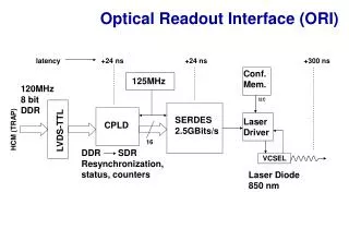
Asynchronous 3Gb/s links Data @ 80MHz Add CRC Low Latency Clock Domain Bridge Data & padding @ 150MHz from Osc-1 3.0 Gb/s Gigabit Transceiver - Tx Gigabit Transceiver - Rx Data & padding @ 150MHz from Osc-2 TTC BC0 Fifo / DualPort RAM remove ‘extra’ comma remove enable Automatic latency synchronisation: Loop over all Fifo locations until Trigger Path BC0 arrives with fixed discrepancy relative to TTC BC0 Data @ 80MHz Check CRC Trigger Workshop: Greg Iles (g.iles@imperial.ac.uk)
Latency: Clk80 to Clk80 data Notes: (a) Latency calculated from clk edge sampling data into SerDes until clk edge exiting SerDes (b) The numbers are obtained from simulation/datasheets and theoretical performance. (c) Assumed 1 write clks (300MHz), 5 read clks (160MHz), If data aligned to slower clock then wait for 1 slow clk to collect all data and up to 1 slow clock to align to slower clock (d) No elastic buffer. Tx = 9.5 x RXUSRCLK, Rx = 10.5 RXUSRCLK (e) Currently bridges from 80MHz to 150MHz in word mode (byte mode would be slightly better). (f) All numbers worst case, but no contingency. (g) Elastic buffer could be removed, albeit with some extra complexity in the VHDL. Trigger Workshop: Greg Iles (g.iles@imperial.ac.uk)
Matrix Card compatibility Drop In Code OGTI card and Matrix card both use Xilinx Virtex5 LX11 0T Current links use existing GCT protocol. May want to change for SLHC. Matrix Card Trigger Workshop: Greg Iles (g.iles@imperial.ac.uk)
Quiet Regions & MIP bits Trigger Workshop: Greg Iles (g.iles@imperial.ac.uk)
Old Design: Quiet Regions & MIP bits RCT RPC/CSC/DT GCT:Source Cards (ECL to optical fibre) uTCA Crate (3x Matrix & CopperLink card) PSB PSB PSB GCT:Main Crate (Data processing) GMT GTI PSB PSB GT Trigger Workshop: Greg Iles (g.iles@imperial.ac.uk)
New Design: Quiet Regions & MIP bits RCT RPC/CSC/DT GCT:Source Cards (ECL to optical fibre) PSB-O PSB-O PSB-O GCT:Main Crate (Data processing) GMT OGTI PSB-O PSB-O GT Trigger Workshop: Greg Iles (g.iles@imperial.ac.uk)
GCT-GT links • Ran all 16 links overnight using different Rx/Tx 100MHz oscillators • No errors ~ 1015 bits • Integrated into GCT hardware • Vienna about to manufacture a new PSB to provide an interface to the GT. • Ready to manufacture final boards Trigger Workshop: Greg Iles (g.iles@imperial.ac.uk)
Extra Trigger Workshop: Greg Iles (g.iles@imperial.ac.uk)
Latency Baseline Current Notes: (a) Latency calculated from clk edge sampling data into SerDes/FPGA until FPGA fabric (b) The numbers are obtained from datasheets and theoretical performace. (c) Assumed 1.0 bx here, but could be 2.0 depending on sync method. (d) No elastic buffer. Tx = 9.5 x RXUSRCLK, Rx = 10.5 RXUSRCLK (e) Assumed ¼ bx for IOB + 2 link speed clks (4 x ½). Based on current 80MHz to 100MHz bridge. (f) All numbers worst case, but no contingency. (g) block ram performance dependent. Trigger Workshop: Greg Iles (g.iles@imperial.ac.uk)
PCB Used 14 layers simply to make routing easier > 320 I/O Routing high speed differential pairs was not that nice. Trigger Workshop: Greg Iles (g.iles@imperial.ac.uk)