Download
1 / 3
30 likes | 102 Views
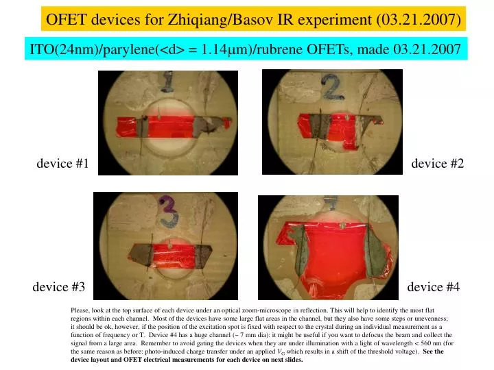
OFET devices for Zhiqiang/Basov IR experiment (03.21.2007). ITO(24nm)/parylene(<d> = 1.14 m )/rubrene OFETs, made 03.21.2007. device #1. device #2. device #3. device #4.

E N D
OFET devices for Zhiqiang/Basov IR experiment (03.21.2007) ITO(24nm)/parylene(<d> = 1.14m)/rubrene OFETs, made 03.21.2007 device #1 device #2 device #3 device #4 Please, look at the top surface of each device under an optical zoom-microscope in reflection. This will help to identify the most flat regions within each channel. Most of the devices have some large flat areas in the channel, but they also have some steps or unevenness; it should be ok, however, if the position of the excitation spot is fixed with respect to the crystal during an individual measurement as a function of frequency or T. Device #4 has a huge channel (~ 7 mm dia): it might be useful if you want to defocus the beam and collect the signal from a large area. Remember to avoid gating the devices when they are under illumination with a light of wavelength < 560 nm (for the same reason as before: photo-induced charge transfer under an applied VG which results in a shift of the threshold voltage). See the device layout and OFET electrical measurements for each device on next slides.
Device layout This is a silver patch coated with parylene; it is only for the purpose of a better fixation of the crystal to the substrate. Not for contacting! 24 nm ITO gate. 20-m gold wires (Source, Drain and Gate); they are bare wires, so you do not need to strip parylene off them. Gate Hard plastic substrate 15mmx15mm and 1 mm thick with an orifice. 50-m gold wires (Source and Drain); they are extending from the graphite electrodes to the silver pads on the substrate. Since the crystal is not glued to the substrate, these thicker and relatively stiffer wires help to hold the crystal sturdy. The Drain wire runs across the crystal, and it is attached to the substrate by two silver pads and to the crystal by the graphite contact. Besides being the Drain contact, it serves as a “clamp” that holds the crystal down to the substrate. Exposed silver pads corresponding to the Gate, Source and Drain (not coated with parylene); can be used for contacting. Source Drain
Transconductance measurements of these OFETs: no leaks or other problems found