Download
1 / 19
190 likes | 201 Views
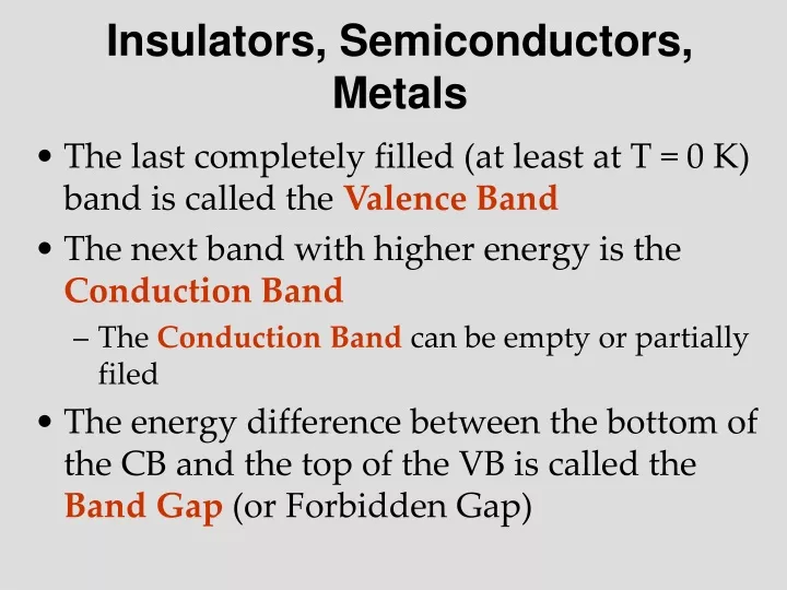
Insulators, Semiconductors, Metals. The last completely filled (at least at T = 0 K) band is called the Valence Band The next band with higher energy is the Conduction Band The Conduction Band can be empty or partially filed

E N D
Insulators, Semiconductors, Metals • The last completely filled (at least at T = 0 K) band is called the Valence Band • The next band with higher energy is the Conduction Band • The Conduction Band can be empty or partially filed • The energy difference between the bottom of the CB and the top of the VB is called the Band Gap (or Forbidden Gap)
Computer simulation can give exact solution in simple cases • Can be found using computer • In 1D computer simulation of light in a periodic structure, we found the frequencies and wave functions • Allowed modes fall into quasi-continuous bands separated by forbidden bands just as would be expected from the tight binding model
Consider a solid with the empty Conduction Band If apply electric field to this solid, the electrons in the valence band (VB) cannot participate in transport (no current) Insulators, Semiconductors, Metals
Insulators, Semiconductors, Metals • The electrons in the VB do not participate in the current, since • Classically, electrons in the electric field accelerate, so they acquire [kinetic] energy • In QM this means they must acquire slightly higher energy and jump to another quantum state • Such states must be available, i.e. empty allowed states • But no such state are available in the VB! This solid would behave as an insulator
Consider a solid with the half filled Conduction Band (T = 0K) If an electric field is applied to this solid, electrons in the CB do participate in transport, since there are plenty of empty allowed states with energies just above the Fermi energy This solid would behave as a conductor (metal) Insulators, Semiconductors, Metals
Band Overlap • Many materials are conductors (metals) due to the “band overlap” phenomenon • Often the higher energy bands become so wide that they overlap with the lower bands • additional electron energy levels are then available
Band Overlap • Example: Magnesium (Mg; Z =12): 1s22s22p63s2 • Might expect to be insulator; however, it is a metal • 3s-band overlaps the 3p-band, so now the conduction band contains 8N energy levels, while only have 2N electrons • Other examples: Zn, Be, Ca, Bi
Band Hybridization • In some cases the opposite occurs • Due to the overlap, electrons from different shells form hybrid bands, which can be separated in energy • Depending on the magnitude of the gap, solids can be insulators (Diamond); semiconductors (Si, Ge, Sn; metals (Pb)
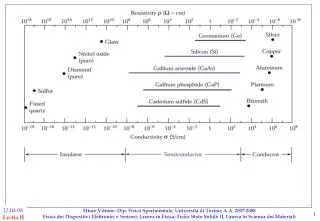
Insulators, Semiconductors, Metals • There is a qualitative difference between metalsandinsulators(semiconductors) • the highest energy band “containing” electrons is only partially filled for Metals (sometimes due to the overlap) • Thus they are good conductors even at very low temperatures • The resisitvity arises from the electron scattering from lattice vibrations and lattice defects • Vibrations increases with temperature higher resistivity • The concentration of carriers does not change appreciably with temperature
Insulators, Semiconductors, Metals • The difference betweenInsulatorsandSemiconductorsis “quantitative” • The difference in the magnitude of the band gap • Semiconductors are “Insulators” with a relatively small band gap • At high enough temperatures a fraction of electrons can be found in the conduction band and therefore participate in transport
Insulators vs Semiconductors • There is no difference between Insulatorsand Semiconductors at very low temperatures • In neither material are there any electrons in the conduction band – and so conductivity vanishes in the low temperature limit
Insulators vs Semiconductors • Differences arises at high temperatures • A small fraction of the electrons is thermally excited into the conduction band. These electrons carry current just as in metals • The smaller the gap the more electrons in the conduction band at a given temperature • Resistivity decreases with temperature due to higher concentration of electrons in the conduction band
Holes • Consider an insulator (or semiconductor) with a few electrons excited from the valence band into the conduction band • Apply an electric field • Now electrons in the valence band have some energy sates into which they can move • The movement is complicated since it involves ~ 1023 electrons
Concept of Holes • Consider a semiconductor with a small number of electrons excited from the valence band into the conduction band • If an electric field is applied, • the conduction band electrons will participate in the electrical current • the valence band electrons can “move into” the empty states, and thus can also contribute to the current
Holes from the Band Structure Point of View • If we describe such changes via “movement” of the “empty” states – the picture can be significantly simplified • This “empty space” is a Hole • “Deficiency” of negative charge – holes are positively charged • Holes often have a larger effective mass (heavier) than electrons since they represent collective behavior of many electrons
Holes • We can “replace” electrons at the top of eth band which have “negative” mass (and travel in opposite to the “normal” direction) by positively charged particles with a positive mass, and consider all phenomena using such particles • Such particles are called Holes • Holes are positively charged and move in the same direction as electrons “they replace”
Hole Conduction • To understand hole motion, one requires another view of the holes, which represent them as electrons with negative effective mass • To imagine the movement of the hole think of a row of chairs occupied by people with one chair empty • To move all people rise all together and move in one direction, so the empty spot moves in the same direction
Concept of Holes • If we describe such changes via “movement” of the “empty” states – the picture will be significantly simplified • This “empty space” is called a Hole • “Deficiency” of negative charge can be treated as a positive charge • Holes act as charge carriers in the sense that electrons from nearby sites can “move” into the hole • Holes are usually heavier than electrons since they depict collective behavior of many electrons
Conduction Electrical current for holes and electrons in the same direction