Download
1 / 6

E N D
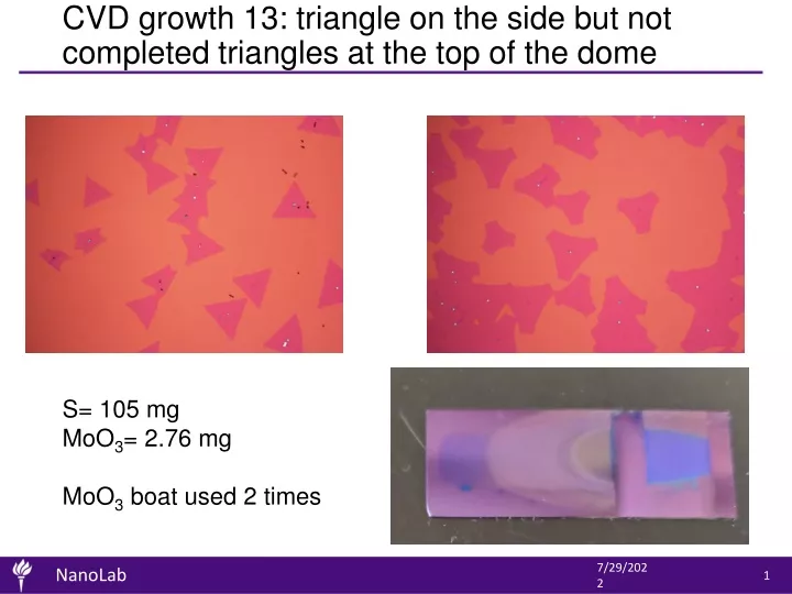
CVD growth 13: triangle on the side but not completed triangles at the top of the dome S= 105 mg MoO3= 2.76 mg MoO3 boat used 2 times
CVD growth 15: around 30/40 mm triangles but with high density of black dots (excess of what?) S= 100.4 mg MoO3= 2.4 mg MoO3 boat used 4 times
CVD growth 16: the quality of MoS2 seems better but smaller triangles S= 103.6 mg MoO3= 2 mg MoO3 boat used 5 times
Raman and PL comparison between CVD 15 and CVD 16 CVD 15 CVD 16
Readout circuit with MoS2. What are the next steps? • Evaluate MoS2 quality measuring various transistors (mobility, SS, Ion/Ioff,..) • Transistors will be transferred on 10 nm Al2O3 trough the Au assisted transfer and contacted with Ni/Au contacts • Once known the performance of the MoS2 transistors perform a back of an envelop calculation such that we can find out the transistor dimensions we will need. • Does the growth allow us to have continuous monolayer regions with these dimensions? • Can we transfer the required MoS2 (needed for the entire circuit) using the Au assisted transfer? • Prepare “drilled” substrates for W bottom gate. Followed by Al2O3 ALD deposition and MoS2 transfer. We will use this structure as a platform to test hundreds of transistors. • One idea to improve the MoS2/Al2O3 interface is to use an HMDS monolayer in between them. Gain access to BNL in order to try this solution
NP_N5A_14 was released, but the shank is still bent • Possible causes of the bent shank: • The square SOI wafer is under strain, causing the probe to bend once released • We observed a not uniform etch (2/3 mm more in the center compared to the head), which caused a not uniform etch of the buried oxide during the bottom etch