Download
1 / 34
390 likes | 435 Views
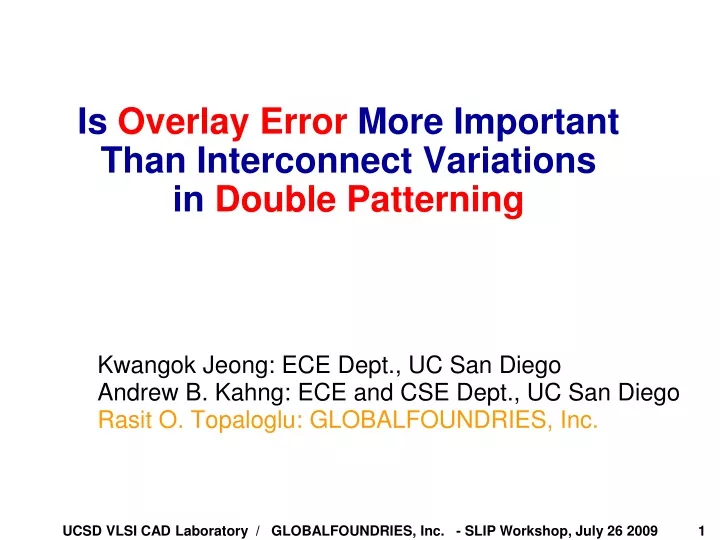
Is Overlay Error More Important Than Interconnect Variations in Double Patterning. Kwangok Jeong: ECE Dept., UC San Diego Andrew B. Kahng: ECE and CSE Dept., UC San Diego Rasit O. Topaloglu: GLOBALFOUNDRIES, Inc. Outline. Traditional BEOL Variation and Process

E N D
Is Overlay Error More Important Than Interconnect Variations in Double Patterning Kwangok Jeong: ECE Dept., UC San Diego Andrew B. Kahng: ECE and CSE Dept., UC San Diego Rasit O. Topaloglu: GLOBALFOUNDRIES, Inc.
Outline • Traditional BEOL Variation and Process • Double Patterning Lithography (DPL) • Overlay Error in Double Patterning • TCAD-Based Analysis • Design-Level Analysis • Conclusions
Outline • Traditional BEOL Variation and Process • Double Patterning Lithography (DPL) • Overlay Error in Double Patterning • TCAD-Based Analysis • Design-Level Analysis • Conclusions
MATERIALS: STEPS: Resist coating Dielectric Mask exposure Cu filling Copper Traditional BEOL Variation and Process • Traditional backend of the line (BEOL) Process • Sources of variation: • Metal/dielectric density- dependent, systematic • Random process variation • Results of variation • Width (W) variation • Metal height (H) variation • Dielectric thickness (D) variation M+1 H M W D M-1 etch
Outline • Traditional BEOL Variation and Process • Double Patterning Lithography (DPL) • Overlay Error in Double Patterning • TCAD-Based Analysis • Design-Level Analysis • Conclusions
Double Patterning Lithography • Double Patterning Lithography (DPL) • Pattern-doubling: ‘2X-resolution’ lithography with traditional ‘1X-resolution’ equipment • Options for double patterning lithography • Process: Double Exposure (DE) / Double Patterning (DP) / Spacer Double Patterning (SDP) • Resist-type: Positive-tone / Negative tone • Target Feature: Line / Spacing Resist 1X Dielectric Mask1 1st Exposure Mask 1X Mask2 2nd Exposure 1X-resolution 2X-resolution
Poly • Spacer-DP • Photoresist • Target Feature (a) Spaces (b) Lines positive resist Cu mask Double Patterning Lithography Options Spacer negative resist hardmask Dielectric • Double Patterning • Double Exposure Target layer Litho-etch & Spacer Formation Litho 1st Litho-etch Etch 2nd Litho-etch Litho-etch (a) Positive-tone (b) Negative-tone
Outline • Traditional BEOL Variation and Process • Double Patterning Lithography (DPL) • Overlay Error in Double Patterning • TCAD-Based Analysis • Design-Level Analysis • Conclusions
Introduction to the Variability in DPL • Overlay error • Causes: • mask misalignment, • material stress-impacted deformations, • litho/etch-impacted topography, • lens aberration, etc. • Results in: • Width variation • Space (or pitch) variation Capacitance variation • Alignment metric • Indirect: • Two DPL masks aligned to a reference layer • Error: • Direct: • Second DPL mask aligned to the first DPL mask • Error: Mask1 Mask2 Reference Direct alignment Indirect alignment S S S S Cc Cg
S S S S S S S Overlay Error in Various DPL Options • Impact on interconnect parameter in DPL options • P (pitch), W (width), W’ W W”,P’ P P’’ 1 2 1 2 1 W’’ W’ P P S/2 Negative DE/DP WIDTH Positive DE/DP SPACE S 1 2 1 2 1 1 2 1 2 1 1 2 1 2 1 W W W’’ W W’ W’ P’ P’’ P P Positive SDP WIDTH & SPACE Negative SDP WIDTH & SPACE P’’ P’
Mask Coloring and Layout Examples in DPL • Mechanism of misalignment-induced variation 2 2 4 4 2 4 4 2 S S 6 6 6 6 1 1 1 1 3 5 3 3 5 5 3 5 Original patterns Coloring Patterns 1 Patterns 2 (a) DE and DP Process Dummy for pattern 6 Spacer (gray) a Narrow space b 2 4 W 1 6 3 5 W” Original patterns Coloring Trim & repair (dark gray) Spacer formation (Large spacer) (b) SDP Process
Outline • Traditional BEOL Variation and Process • Double Patterning Lithography (DPL) • Overlay Error in Double Patterning • TCAD-Based Analysis • Design-Level Analysis • Conclusions
TCAD-Based Analysis Setup • Test structure • Design of experiments (DOE) • Full combinations of W, H, D and S • For all DE/DP/SDP with positive/negative-tone resist • 3 variation: We assume 20% of nominal value M+1 layer D: dielectric height W: line width H: line height S: overlay shift S D H M layer W M-1 layer • 1. for (i = -3 ; i 3 ; i=i+1) { • for (j = -3 ; j 3 ; j=j+1) { • for (k = -3 ; k 3 ; k=k+1) { • for (l = -3 ; l 3 ; l=l+1) { • W=Wnom + iW3 • H= Hnom + jH3 • D= Dnom + kD3 • S = Snom + lS3 • run field solver over • parameterized structure}}} • Find nominal and worst-case capacitance
TCAD-Based Analysis Results • Overlay vs. width vs. height • Indirect alignment shown: • Impact of overlay: 0 ~ 2.4% of C-total • Impact of width: -13% ~ 10% of C-total • Impact of height: -32% ~ 18% of C-total • Impact of indirect alignment ~ 2x direct alignment Capacitance (aF/um)
Outline • Traditional BEOL Variation and Process • Double Patterning Lithography (DPL) • Overlay Error in Double Patterning • TCAD-Based Analysis • Design-Level Analysis • Conclusion
Design-Level Analysis Flow • Overlay-aware extraction flow TOP.GDS AES core with NanGate 45nm Tech. 1. Design GDS Initial GDS 2. Split GDS ILP-based min cost coloring (Kahng et al. ICCAD08) Non-DPL layers 3. Pattern Decomposition DPL layers Sub-GDS1 Base GDS Coloring and Splitting Sub-GDS1-1 Sub-GDS2 Sub-GDS1-2 Sub-GDS2-1 4. Shift and Merge (Cadence Virtuoso) Sub-GDS2-2 Shifting and Merging TOP.GDS 5. Resize and Extraction (Synopsys Hercules, Star-RCXT) Resizing
Design-Level Analysis DOE • Design of Experiments for DE/DP with DA • foreachlayer { M2, M3, M4, M5 } • decompose layer into layermask1 and layermask2 • foreachS { -3/2, -2/2, -/2, 0, /2, 2/2, 3/2} • shift layermask1 by S • shift layermask2 by –S • end • layer layermask1 + layermask2 • foreachW { -3/2, -2/2, -/2, 0, /2, 2/2, 3/2} • resize layer by W • end • merge with other layers • RC-Extraction and Timing Analysis • end
Impact on Capacitance Variation • Total interconnect capacitance: maximum C(%) • Among top 20% high capacitance nets • Impact of overlay < impact of width • Sum of capacitance in the most critical path • Critical path has short interconnects impact of BEOL variation significantly reduces • Impact of overlay < impact of width
Impact on Crosstalk-Induced Delay • Maximum coupling induced delay change • PrimeTime-SI (Synopsys) is used to find a net that is mostly affected due to crosstalk • Temporal/functional filtering is performed • Selected net structure • A net with relatively small length (~17um) can have >10% delay changes due to overlay error M4 segment: 14.788um M2 segment: 1.604um M3 segment: 0.78um Capacitance when Delay is maximum Capacitance when Delay is minimum
- 60 - 50 - 40 - 30 - 20 Overlay Width - 10 0 - 3s - 2s - 1s 0s 1s 2s 3s Interconnect variation Impact on Timing • Longest path and total negative slack (TNS) • Impact of overlay << impact of width • Longest path delay changes negligibly • However, overall timing (TNS) can change significantly Total Negative Slack (ns)
Outline • Traditional BEOL Variation and Process • Double Patterning Lithography (DPL) • Overlay Error in Double Patterning • TCAD-Based Analysis • Design-Level Analysis • Conclusions
Conclusions • We provide a variational interconnect analysis technique for double patterning lithography • We analyze interconnect variations due to overlay error in DPL • We augment previous work by providing both interconnect and chip-level RC-extraction framework reflecting interconnect variation in a 45nm DPL process • We compare the impact of overlay error with traditional interconnect variations • Summary of observations • Indirect alignment results in higher variation than direct alignment • In most analysis, impact of traditional variation source (width) is larger than that of overlay error, however, overlay error is additive and non-negligible • Overlay error can cause up to 10% capacitance variation and 13% increase of crosstalk-induced delay • Ongoing/Future Work • Impact in the presence of metal fills • More in-depth analysis or remaining DPL process options • Process sensitivity analysis
Misalignment Under M1 Layer (Standard-Cell) • Standard cell structure • Assumptions • There exist a reference coordinate to measure misalignment • 10nm misalignment is a maximum displaced distance from the reference coordinate • Possible moves • Poly1: left 10nm (L) / 0nm (C) /right 10nm (R) • Poly2: left 10nm (L) / 0nm (C) /right 10nm (R) • M1: left 10nm (L) / 0nm (C) /right 10nm (R) • Contact: left 10nm (L) / 0nm (C) /right 10nm (R) • All Combinations = 3*3*3*3 = 81 cases • Naming convention for each testcase • P1{direction}_P2{direction}_C{direction}_M{direction} • E.g., “P1C_P2L_CC_MC” means even gates move lef t by 10nm Original P1 P2 M C BASE (a) (b)
Experimental Results on Standard Cell RED: Original Blue: Shift one set of gates Green: Shift M1 and Cont. (same direction)
DPL Options • Spacer-DP • Double Exposure • Double Patterning Mask Resist Resist Resist Hardmask Hardmask Target layer Buffer oxide Target layer Hardmask Target layer Mask1 Mask1 Target layer 1st Litho-etch mask 1st Exposure 1st Litho-etch positive resist Mask2 negative resist Mask2 Spacer formation Oxide depo. CMP 2nd Litho-etch 2nd Exposure Dielectric After exposure & etch 2nd etch Cu interconnect Spacer removal • Printed Feature • Photoresist After Cu filling mask (a) Positive-tone (b) Negative-tone positive resist Dielectric Poly After exposure & etch Cu interconnect Poly (a) Spaces (Trench-First) (b) Lines
S Impact of Overlay in Positive DE/DP mask1 mask2 (misaligned to left) Positive photoresist Dielectric After exposure + etch After filling Cu Cu S 1 2 1 2 1 W W P’ P’’
S S Impact of Overlay in Negative DE/DP mask1 mask2 (misaligned to left) Negative photoresist Dielectric After exposure + etch After filling Cu Cu 1 2 1 2 1 W’’ W’ P P S/2
S S Impact of Overlay in Positive SDP Primary patterns Spacers (act as if masks) (kind of) Positive photoresist Dielectric After exposure + etch After filling Cu Cu 1 2 1 2 1 W’’ W P P
S S Impact of Overlay in Positive SDP Primary patterns Spacers (act as if masks) (kind of ) Negative photoresist Dielectric After exposure + etch After filling Cu Cu 1 2 1 2 1 W’ W’ P’’ P’
Electrical Impacts: Capacitance Variation • Overlay error can cause more than +/- 10% capacitance variation within a die • This variation must be back-annotated to timing analysis to reduce unnecessary guardbanding Capacitance Variation (%)
M2 |S| |S|/2 |S|/2 |S|/2 M4 |S| |S|/2 |S|/2 |S|/2 P-DE/DP N-DE/DP P-SDP N-SDP
Maximum Crosstalk Induced Delay • A net has maximum crosstalk-induced delay • SDP shows more sensitivity tighten overlay spec • P-DE/DP shows least sensitivity lessen overlay spec M4 B A |S| |S|/2 |S|/2 |S|/2 P-DE/DP N-DE/DP P-SDP N-SDP M2 M4 M4 M2 w/o metal fill w/ metal fill
Total Negative Slack Variation • SDP, especially for lower layer (smaller feature), shows more sensitivity tighter overlay spec