Download
1 / 35
350 likes | 510 Views
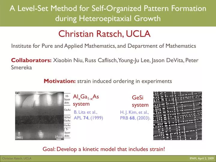
A Level-Set Method for Self-Organized Pattern Formation during Heteroepitaxial Growth. Al x Ga 1-x As system. GeSi system. B. Lita et al., APL 74 , (1999). H. J. Kim, et al., PRB 68 , (2003). Christian Ratsch, UCLA Institute for Pure and Applied Mathematics, and Department of Mathematics.

E N D
A Level-Set Method for Self-Organized Pattern Formation during Heteroepitaxial Growth AlxGa1-xAs system GeSi system B. Lita et al., APL 74, (1999) H. J. Kim, et al., PRB 68, (2003). • Christian Ratsch, UCLA • Institute for Pure and Applied Mathematics, and Department of Mathematics Collaborators: Xiaobin Niu, Russ Caflisch, Young-Ju Lee, Jason DeVita, Peter Smereka Motivation: strain induced ordering in experiments Goal: Develop a kinetic model that includes strain! IPAM, April 2, 2009
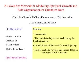
Outline of this Talk • Introduction • The level-set method for epitaxial growth • Spatially varying potential energy surface • (due to surface defects, reconstructions, … ) • Our elastic model • Ordering in the submonolayer growth regime • Ordering of stacked quantum dots IPAM, April 2, 2009
What is Epitaxy? epi - taxis above Arrangement (in ordered manner) Application: many microelectronic devices (example shown: suggestion for a quantum repeater) A Gates J Gates Read-out Channel Depletion Gate (1 of 2) i-InP n+InP i-InP i-Ga0.58In0.42As Qubit Layer i-InP i-Ga0.60In0.40As Read-out Layer i-InP n+InP i-InP Wikipedia: The term epitaxy describes an ordered crystalline growth on a (single-) crystalline substrate. It involves the growth of crystals of one material on the crystal face of another (herteroepitaxy) or the same (homoepitaxy) material. The lattice structure and orientation or lattice symmetry of the thin film material is identical to that of the substrate on which it is deposited. IPAM, April 2, 2009
Physical Processes During Epitaxial Growth IPAM, April 2, 2009
Hierarchy of Theoretical Approaches Time Continuum Methods Device growth Hybrid Methods (Level Set) 1s Statistical Methods (KMC) 1ms Formation and growth of islands Molecular Dynamics 1ms Atomic motion 1ns QM (DFT) Vibrations of atoms 1ps 1nm 1m 1mm 1mm length wafers islands atoms devices IPAM, April 2, 2009
KMC Simulation of a Cubic, Solid-on-Solid Model F D = G0 exp(-ES/kT) Ddet = D exp(-EN/kT) Ddet,2 = D exp(-2EN/kT) ES: Surface bond energy EN: Nearest neighbor bond energy G0 : Prefactor [O(1013s-1)] • Parameters that can be calculated from first principles (e.g., DFT) • Completely stochastic approach IPAM, April 2, 2009
KMC Simulations: Effect of Nearest Neighbor Bond EN More Detailed KMC model InAs(100) Ni/Ni(100) Au/Ru(100) Kopatzki et al., Surf.Sci. 284 (1993) F. Grosse et al. PRL 89 (2002) Hwang et al., PRL 67 (1991) Large EN: Small EN: IPAM, April 2, 2009
The challenge for including strain in a growth model • Strain calculations for a system of typical size in 2+1 dimensions are expensive (at least seconds, maybe minutes) • A typical timestep in an atomistic simulation is of order 10-6 seconds (which is the inverse of a typical diffusion constant D=106.) • Need of the order of 1 million timesteps (or more) to simulate 1 second • Possible solutions to this challenge • 1) Don’t solve global elastic field at every timestep • solve it only locally, maybe not even every timestep • do only occasional global updates. • 2) Develop a model where the simulation timestep can be taken much larger, but where still all the microscopic dynamics are retained. • We have developed a level set method • Typical timestep in the simulation is of order 10-2 seconds. IPAM, April 2, 2009
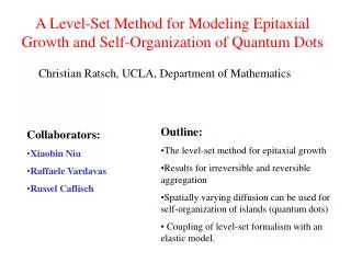
Outline of this Talk • Introduction • The level-set method for epitaxial growth • Spatially varying potential energy surface • (due to surface defects, reconstructions, … ) • Our elastic model • Ordering in the submonolayer growth regime • Ordering of stacked quantum dots IPAM, April 2, 2009
The Island Dynamics Model for Epitaxial Growth Island dynamics Atomistic picture(i.e., kinetic Monte Carlo) F v D • Treat Islands as continuum in the plane • Resolve individual atomic layer • Evolve island boundaries with levelset method • Treat adatoms as a mean-field quantity (and solve diffusion equation) IPAM, April 2, 2009
The level set method: schematic • Governing Equation: j=0 j=0 j=1 j=0 Level set functionj Surface morphology j=0 t • Level set function is continuous in plane, but has discrete height resolution • Adatoms are treated in a mean field picture IPAM, April 2, 2009
The Level Set Method is diffusion matrix. • Diffusion equation: • Boundary condition: Diffusion in x-direction Diffusion in y-direction • Velocity: Ñ + Ñ drift ~ D E D E xx x ad yy y ad A typical potential energy surface : Adatom concentration Etrans Nucleation rate ~ detachment rate Ead Edetach • Stochastic element needed for nucleation IPAM, April 2, 2009
A typical level set simulation IPAM, April 2, 2009
Outline of this Talk • Introduction • The level-set method for epitaxial growth • Spatially varying potential energy surface • (due to surface defects, reconstructions, … ) • Our elastic model • Ordering in the submonolayer growth regime • Ordering of stacked quantum dots IPAM, April 2, 2009
Assume spatially varying potential energy surface (no strain) Experiment by Xie et al., UCLA Interpretation: Variation of potential energy surface is due to strain, that results from burried defect lines Etrans Ead IPAM, April 2, 2009
Variation of adsorption and transition energy Kinetic limit Thermodynamic limit Etrans Etrans Ead Ead Nucleation in region of slow diffusion (but high adatom concentration), dominated by drift Nucleation in region of fast diffusion Nucleation rate ~ IPAM, April 2, 2009
Ordering by Cleaved Edge Overgrowth (a) (b) Grow AlAs/GaAs superlattice Cleave and rotate Grow InAs quantum dots Quantum dots grow on top of the AlAs stripes Work of E. Uccelli, G. Abstreiter, et al. Width of AlAs stripe: 30 nm 42 nm 80 nm 100 nm IPAM, April 2, 2009
Level set simulations Nucleation rate as function of position for increasing width of AlAs stripe Etrans Ead IPAM, April 2, 2009
Outline of this Talk • Introduction • The level-set method for epitaxial growth • Spatially varying potential energy surface • (due to surface defects, reconstructions, … ) • Our elastic model • Ordering in the submonolayer growth regime • Ordering of stacked quantum dots IPAM, April 2, 2009
Include Strain: Calculate Elastic Field at Every Timestep • Our Model: Write down an atomistic energy density, that includes • Nearest neighbor springs Diagonal springs • This can be related to (and interpreted as) continuum energy density • Minimize energy with respect to all displacements: u E [u] = 0 • The relevant microscopic parameters at every grid point can then be varied as a function of the local strain. IPAM, April 2, 2009
How does Strain affect the Parameters in our Model? GaAs(100) (a semiconductor) E. Penev et al., Phys. Rev. B 64, 085401 (2001). Density-functional theory (DFT) has been used to study strain dependence of surface diffusion D Ag/Ag(111) (a metal) Etrans Ead Energy barrier for surface diffusion Ratsch et al. Phys. Rev. B 55, 6750-6753 (1997). IPAM, April 2, 2009
Dimer Dissociation and Detachment for Ag/Ag(100) Dimer dissociation Adatom detachment Preliminary DFT Results suggest decrease of energy barrier for dimer dissociation and adatom detachment upon tensile and compressive strain: Tests show that the dependence of Ddet is more important for ordering of island sizes, while dependence of D is more important for ordering of location. IPAM, April 2, 2009
Effect of Strain in the Simulation Adatom concentration morphologies Elastic energies IPAM, April 2, 2009
Effect of Strain in the Simulation Morphologies Elastic energies Detachment rate Adatom concentration Top row: Strain=1% Bottom row: Strain=5% • With increasing strain, islands become more regular, because small islands are more likely to break up, and growth of large islands slows down. IPAM, April 2, 2009
Sharpening of the Scaled Island Size Distribution Experiment: InxGa1-xAs/GaAs(100) 7% misfit 4.7% misfit 2.3% misfit D. Leonard, M. Krishnamurthy, S. Fafard, J.L. Merz, and P.M. Petroff, J. Vac. Sci. Tech B 12, 1063 (1994) Level-set simulation IPAM, April 2, 2009
Outline of this Talk • Introduction • The level-set method for epitaxial growth • Spatially varying potential energy surface • (due to surface defects, reconstructions, … ) • Our elastic model • Ordering in the submonolayer growth regime • Ordering of stacked quantum dots IPAM, April 2, 2009
Simulation of Stacked Quantum Dots AlxGa1-xAs system Experimental observation: Stacked quantum dots align under certain conditions Question/goal: can we understand and model this, and make some predictions and suggestions? B. Lita et al., APL 74, (1999) IPAM, April 2, 2009
Simulation of Stacked Quantum Dots b a a b a Repeat Capping and Growth of N Super layers n capping layers of Si Ge Si Substrate • Growth of islands on substrate without strain (constant diffusion and detachment) • Fill in capping layer “by hand” • Calculate strain on top of smooth capping layer • Modify microscopic parameters for diffusion and detachment) according to strain • Run growth model • Repeat procedure IPAM, April 2, 2009
Ordering of stacked quantum dots AlxGa1-xAs system B. Lita et al., APL 74, (1999) • Spacing and size of stacked dots becomes more regular X. Niu, Y.-J. Lee, R.E. Caflisch, and C. Ratsch,Phys. Rev. Lett. 101, 086103 (2008). IPAM, April 2, 2009
Simulation of growth of 20 superlayers IPAM, April 2, 2009
Regularization of dot size IPAM, April 2, 2009
Ordering of stacked quantum dots (top view) Growth of stacked quantum dots of In0.5Ga0.5As/GaAs(100) 2 periods 9 periods 7 periods V.V. Strel’chuk et al., Semiconductors 41 (2007) IPAM, April 2, 2009
Thickness dependence of vertical ordering 4 capping layers 0 capping layer 2 capping layers • We find an optimal thickness of capping layer for ordering IPAM, April 2, 2009
Nucleation rate as a function of capping layer thickness 60 30 60 IPAM, April 2, 2009
Conclusions • We have developed a numerically stable level-set method to model epitaxial growth • A spatially varying potential energy surface can be exploited to obtain ordered structures. • It is very efficient to include strain in the model, and solve the elastic equations at every numerical timestep. • Strain leads to ordering in the submonolayer growth regime • We model the formation and self organization of stacked quantum dots, and suggest that an optimal thickness exists. IPAM, April 2, 2009