Download

1 / 20

E N D
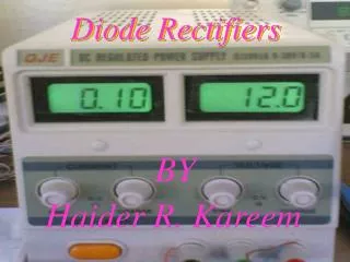
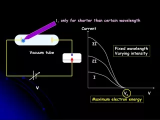
INTRODUCTION For reasons associated with economics of generation and transmission, the electric power available is usually an a.c. supply. The supply voltage varies sinusoidally and has a frequency of 50 Hz. It is used for lighting, heating and electric motors. But there are many applications where d.c. supply is needed. When such a d.c. supply is required, the mains a.c supply is rectified by using vacuum diodes. A vacuum diode can do rectification due to unidirectional conduction i.e. it will conduct current only when plate is positive w.r.t. cathode. Although vacuum diodes have been upstaged by crystal diodes as rectifiers, they are still used in many applications.
Types of Vacuum Tube Rectifiers - Broadly, single phase vacuum tube rectifiers may be classified into half-wave rectifier and full-wave rectifier. It is usual practice to give a.c supply for rectification through a transformer. There are two reasons for it. First, a transformer allows us to step up or down thea.cvoltage. Second, it isolates the rectifier circuit from power lines and thus reduces the risk of electric shock.
Half-wave rectifier • A half-wave rectifier employs a single diode and conducts current during the positive half-cycles of input a.csupply are suppressed i.e. During negative half-cycles, no current is conducted and hence no voltage appears across the load. Therefore, current always flows in one direction (i.e. d.c.) through the load, though after every half-cycle.
Suppose an a.c. Supply v = Vm sin 0 is applied to a half-wave rectifier. Let rp and RL be the diode resistance and load resistance respectively. Then the various circuit computations will be :
Full-wave Rectifier • A full-wave rectifier employs at least two diodes and conducts current through the load in the same direction for both half cycles of input a.c. Voltage. For the positive half-cycle of a.c. Voltage, one diode supplies current to the load and for the negative half-cycle, the other does so; the current being always in the same direction through the load. Therefore, a full-wave rectifier utilises both half-cycles of
Input a.c. Voltage to produce the d.c. Output. The circuits commonly used for full-wave rectification are: a. Centre-tap circuit b. Bridge circuit
Suppose an a.c. Supply v = Vm sin 0 is applied to a full-wave rectifier. Then the various circuit computations are: Efficiency of rectification
It is clear that for a given a.c. Supply, the output of a full-wave rectifier is double than that of a half-wave rectifier. For this reason, full-wave rectifiers are invariably used for conversion of a.c. Into d.c.
Peak Inverse Voltage (PIV) • It is the maximum reverse voltage that can be applied to a vacuum diode without damage to it. The PIV consideration is of particular importance in rectifier service. While using a diode for rectification, care should be taken that reverse voltage across the diode during negative half-cycle of a.c. Supply does not exceed the PIV reting of the diode.
Basic Electronics Semiconductor Physics
Introduction Certain substances like germanium, silicon etc. are neither good conductors like copper nor insulators like glass. In other words, the resistivity of these materials lies in between conductors and insulators. Such substances are called semi-conductors. In fact, it is not the resistivity alone that decides whether a substances is semi-conductor or not. They have several unique properties which distinguish them from conductors and insulators. One very important property of semi-conductors is that with the addition of suitable metallic impurity ( e. g. arsenic, gallium etc.) to a semi-conductor, it’s conducting properties change appreciably. This property is the key factor responsible for the widespread use of semi-conductors in the electronic devices. A large number of semi-conductor are known but the most commonly used are silicon (Si) and germanium (Ge). Both these elements are tetravalent i.e they have four valence electrons. The different atoms of a semi-conductors are held together in an orderly pattern through co-valent bonds. Therefore, a piece of germanium or silicon is generally called a crystal
Intrinsic semi-conductor A semi-conductor in an extremely pure form is called an intrinsic semi-conductor. Even at room temperature some of the co-valentbonds in a pure semi-conductor break, setting up free electrons. When aco-valent bond is broken due to thermal energy, the removal of one electrons leaves a vacancy i.e. a missing electron in the co-valent bond. This missing electron is called a hole. For one electron set free, one hole is created. Therefore, there energy creates hole-electron pairs; there being as many holes as the free electrons. When electric f field is applied across a pure semi-conductor, the current conduction takes place by free electrons and holes . The total current inside the semi conductor is the sum of currents due to free electrons and holes.
Extrinsic semi-conductor The intrinsic semi-conductor has little current conduction capability at room temperature. To be useful in electronic devices, the pure semi-conductor must be altered so as to significantly increase its conducting properties. This is achieved by adding a small amount of suitable metallic impurity to pure semi-conductor. It is then called an impure or extrinsic semi-conductor. The purpose of adding impurity is to increase either the number of free electrons or holes in the semi-conductors crystal. (i) If a pentavalent impurity (i.e having 5 valence electrons) is added to a pure semi-conductor, a large number of free electrons are produced in the semi-conductor. The semi-conductor thus produced is known as n-type semi-conductor. Although there are some holes in an n-type due to thermal energy, yet the number of free electrons far outnumber the holes . Therefore. The current conduction in an n-type semi –conductor is predominantly by free electrons. It is customary to call the free electrons in n-type as the majority carriers and holes as the minority carriers and holes as the minority carriers. (ii) If a trivalent impurity( (having 3 valence electrons) is added to a pure semi-conductors, a large number of holes are produced in the semi-conductor. Although there will be some free electrons in a p-type semi-conductor due to thermal energy, yet the number of holes far exceeds the free electrons. Therefore, current conduction in a p-type semi-conductor is predominantly by hole. It is obvious that in a p-type semi-conductors holes are the majority carriers while free electrons are the minority carriers.
Pn Junction When a p-type semi-conductor is suitably joined to n-type semi-conductor, the contact surface is called a pnjunction, Most of semi-conductor devices contain one or more pn junctions. As soon as a pn junction is formed, there is tendency for the free electrons to diffuse over to junction I is formed , there is tendency for the free electrons to diffuse over to p-side and holes to n-side. This diffusion process sets up a potential barrier at the junction which prevents the further movement of charge carriers ( i.e. holes and free electrons) across the junction, for germanium junction, the value of this potential barrier is 0.3 V whereas it is 0.7 V for silicon pn junction. • When external voltage applied to the pn junction is such that it cancels the potential barrier, thus permitting current flow, it is called forward biasing. In order to forward bias a pnjunction. Connect positive terminal of battery to p-type and negative terminal to n-type. As potential barrier voltage is very small, therefore, a small forward voltage is sufficient to completely eliminate the barrier. • When external voltage applied to a pn junction is such that potential barrier is increased, it is called reverse biasing. In order to reverse bias a pnjunction, connect positive terminal of battery to n-type and negative terminal to p-type. No can flow across a reverse biased pn junction showing that it offers very high resistance
BSE-tle iii Engr. AquilinoNoceda