Download
1 / 21
210 likes | 313 Views
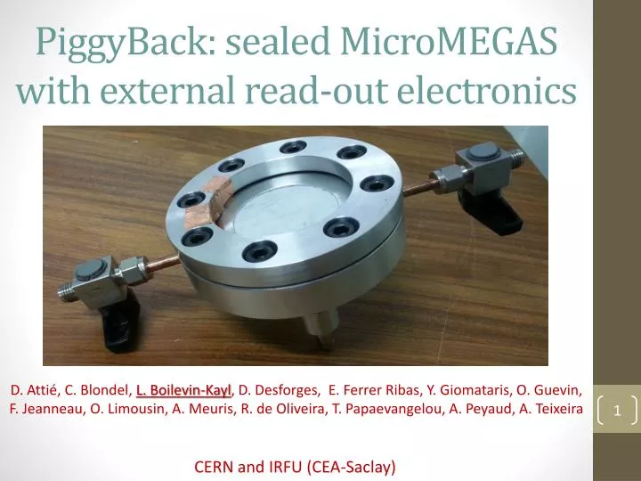
PiggyBack : sealed MicroMEGAS with external read -out electronics. D. Attié , C. Blondel, L. Boilevin -Kayl , D. Desforges , E. Ferrer Ribas , Y. Giomataris , O. Guevin , F. Jeanneau, O. Limousin, A. Meuris , R. de Oliveira, T. Papaevangelou , A. Peyaud , A. Teixeira.

E N D
PiggyBack: sealedMicroMEGASwithexternalread-out electronics D. Attié, C. Blondel, L. Boilevin-Kayl, D. Desforges, E. Ferrer Ribas, Y. Giomataris, O. Guevin, F. Jeanneau, O. Limousin, A. Meuris, R. de Oliveira,T. Papaevangelou, A. Peyaud, A. Teixeira CERN and IRFU (CEA-Saclay)
Outline and statut report Motivation and reminder of previouspresentation Characterization of the new chamber in normal and sealedoperation Characterization of new bulks Set-upwith new high-tech read-out electronics First results of the coupling to electronics Conclusions and outlook
Why ? To reducesparking and to protect the detector Reminder: resistiveMicroMEGAS How ? Thinresistive layer deposited on an adequateinsulator Resistivethin layer 1MΩ/□ to 100 GΩ/□ Standard bulk structure Development of PiggyBackresistiveMicroMEGAS Insulator: Ceramicsubstrate thickness ≃ 100-500 µm Detector dissociatedfromread-out plane, sowhy not : Read-out plane Couple it to ≠ electronics ? Work in sealedoperation ?
Reminder: evolution of PiggyBack • HV connectorsoutside • Ceramicpartiallyoutside • Made in aluminium • PCB Boardunderceramic layer • HV connectorsinside • Ceramictotallyinside • Made in stainlesssteel • Uncoveredceramic layer Verify the resistive layer concept Good performances in normal mode Verylowoutgassing Robust and versatile
Mesh Bulktechnology on ceramic 2 mm Resist 50 mm Ground ≃ 1 or 2 cm Vmesh ≃ 128 µm Va ≃ 5-25 µm ≃ 100-500 µm Read-out Amplification fielddepends on two voltages!
Anode Mesh Set-up Fe55 Source Electronics Data processing Performance expected: • Electron transparency: a large flat curvewhere gain ≥ 95% of max gain • Gain ≥ 104 • Energyresolution: ≃ 20-26% (for 5.9 keV) And the most important one: good stability of gain for severaldays!!!
Evolution of the position of the main peakwith the electrical ratio • Fixed amplification field, evolving drift field Electron transmission
Keepworkingwith voltages verifyingthe optimizedtransmission • Increase gain until apparition of sparks Electron gain
Relation used : with E = 5.9 keV • Fit with ROOT, considering the twogaussiansfrom Argon spectrum Energyresolution
Characterization Expected performance Achieved performance End performance characteristics A large flat curvewhere gain ≥ 95% of max gain Widthfrom a ratio of 0.001 to 0.015 Gain ≥ 104 Gain ≥ 2.104 Energyresolution≤ 25% for a large range of amplification fields Energyresolution≤ 26% The new chambermeets the expected performance in normal operation
Evolution of gain and energyresolutionduringseveraldays: • Important gasleaks Stability in sealedoperation • Solutions: • Torr Seal glue on HV connectors • New nuts for the mechanics The new chamberisnowleak-proof enough
Environmentalstudy Adloff et al., Environmentalstudy of a Micromegas detector Wecannotneglect the evolutionsinduced by the environment
Low noise, very good resolution, radiation hardness, lowcost,… • Couldwork at normal and high temperature • Improved performance for space missions Coupling to high-tech electronics How? Put the electronics at the bottom of the ceramic layer Signal transmission by capacitive transmission Why? ? ¿ High-tech electronics ? ¿
Read-out in 256 pixels No dead-space Made of 8 eightprogrammable ASICs A powerful detector camera: Caliste Detector above made in CdTe Very compact and robuste Optimised for space missions
Architecture of one IDeF-XHD ASIC: For eachchannel:low noise/low charge preamplifier + sharperwithadjustablepeaking time + discriminator to set the lowthreshold value + peak detector to memorize the pulse height And its front-end electronics Signal induced in pixels trigger set up and sent to SAB. FPGA beginsreadoutsequencechannel by channel : date, adress, energy Sequel of actions: + FPGA card + SAB card • In permanent reconfiguration withlogicalgates • Userscommunicatewiththe card by scripts • Communication between the electronics and the computer
Test withstopped signal: two breaks (40s-50s and 80s-100s) withfixed amplitude (10mV) Injection of signals in one ASIC Test withvarioussignal: modification of the amplitude (20, 10 and 15mV) after the breaks
Calistecard Interface Set up of couplingelectronics Caliste Detector FPGA card Fe55 Vessel Computer Data processing
First results on coupled detector Weget the spectrum of the iron source! Center of the source First time thatMicroMEGAS are successfullycoupled to spaceelectronics!
ResistiveMicroMEGASwere compatible withread-out electronics • This couplingisworkingthanks to capacitive transmission • Signalsfrom a pulser have been successfullyinjected and observed • First picture of the iron source acquired! Conclusions and outlook Possibility to build up an imagingspectrometer in the soft X-ray domain! So, maybe, in the future,… World of detection Physics of detectors Development of electronics
Thankyou for your attention Any question?
ResistiveMicroMEGAS and PiggyBack: • A PiggybackresistiveMicromegas • Attié, D.; Chaus, A.; Colas, P.; Ferrer Ribas, E.; Galan, J.; Giomataris, I.; Iguaz, F.J.; Gongadze, A.; De Oliveira, R.; Papaevangelou, T.; Peyaud, A. • JINST (2013) 8 C11007 • Environmentalstudy: • Environmentalstudy of a Micromegas detector • Adloff, C.; Chefdeville, M.; Espargilière, A.; Gaglione, R. • LAPP-TECH-2009-03 • Caliste HD: • CalisteHD: A new fine pitch Cd(Zn)Te imagingspectrometerfrom 2 keV up to 1 MeV • Meuris, A.; Limousin, O.; Gevin, O.; Lugiez, F.; Le Mer, I.; Pinsard, F.; Donati, M.; Blondel, C.; Michalowska, A.; Delagnes, E.; Vassal, M.-C.; Soufflet, F., • IEEE NUCLEAR SCIENCE SYMPOSIUM - CONFERENCE RECORD, 2011 • IDeFX-HD: • IDeF-X HD: A low power multi-gain CMOS ASIC for the readout of Cd(Zn)Te detectors • Michalowska, A.; Gevin, O.; Lemaire, O.; Lugiez, F.; Baron, P.; Grabas, H.; Pinsard, F.; Limousin, O.; Delagnes, E. • IEEE NUCLEAR SCIENCE SYMPOSIUM - CONFERENCE RECORD, 2010 References