Download
1 / 28
470 likes | 1.53k Views
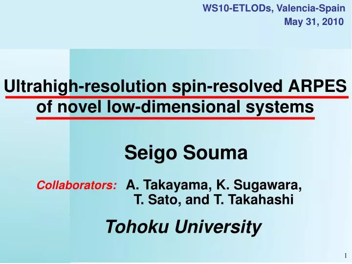
WS10-ETLODs, Valencia-Spain. May 31, 2010. Ultrahigh-resolution spin-resolved ARPES of novel low-dimensional systems. Seigo Souma. A. Takayama , K. Sugawara, T. Sato, and T. Takahashi. Collaborators:. Tohoku University. Rashba effect. Topological insulator. Spintronics.

E N D
WS10-ETLODs, Valencia-Spain May 31, 2010 Ultrahigh-resolution spin-resolved ARPES of novel low-dimensional systems Seigo Souma A. Takayama, K. Sugawara, T. Sato, and T. Takahashi Collaborators: Tohoku University
Rashba effect Topological insulator Spintronics Rashba term Spin-orbit interaction Electronic-field induced spin-current Bi2Te3 Anomalous electron spin phenomena Spin switch via S.O. interaction Y.L.Chenet al., Science 325 (2009) 178. Edge state (surface state) Time reversal invariant E(k,↑) = E(-k,↓) Spin dependence of electronic structure High-resolution spin-resolved ARPES
Spin-splitting of surface Rashba effect Surface Rashba effect Time reversal symmetry Space inversion symmetry E(k,↑) = E(-k,↓) E(k,↑) = E(-k,↑) Spin-orbit interaction ∇V= (0, 0, Ez) surface potential Effective magnetic field spin-resolved ARPES
Angle-resolved PES (ARPES) e-freedom • Energy • Momentum
Mott scattering Spin-resolved ARPES Detection of electron spin is difficult !! 25 keV e-freedom • Energy • Momentum Mini Mott Detector • Spin Efficiency of instrument goes down by 3-4 order Energy Resolution 100 meV
Recent spin-resolved ARPES studies [7,8] [4,5] [1,2] c Mott detector Mott detector VLEED (retarding-type) (high-energy type) (Fe(001)p(1x1)-O) Electron diffraction EK = 6 eV Mott scattering EK = 60 keV Mott scattering EK = 25 keV [3] [9] [6] Sb(111) Au(111) Bi1-xSbx(x=0.13) DE = 70 meV DE = 70 meV DE = 30 meV [1] K. Iori et al., RSI 77 (2006) 013101. [4] V. N. Petrov et al., RSI 68 (1997) 4385. [7] R. Bertacco et al., RSI 73 (2002) 3867. [2] S. Qiao et al., RSI 68 (1997) 4390. [5] M. Hoesch et al., JESRP 124 (2002) 263. [8] T. Okuda et al., RSI 79 (2008) 123117. [3] T. Kadono et al., APL 93 (2008) 252107. [6] M. Hoesch et al., PRB 69 (2004) 241401(R). [9] A. Nishide et al., PRB 81 (2010) 041309(R).
Spin-resolved ARPES system Spin-integrate ARPES Angle Energy Spin-resolved ARPES spin up D B spin down Spin polarization z Pz (A,B) Py y A C (C,D) x
Energy resolution at MCP metal superconductor Au Nb T = 3.5 K Tc = 9.2 K Xe I 8.437 eV T = 3.5 K Xe I 8.437 eV simulation simulation BCS function FD function Gap size D = 1.5 meV Broadening G = 200 meV Energy resolution at MCP 900 meV
Ep: pass energy High-resolution spin-resolved photoemission spectrometer Energy resolution @ Mott ~ 0.008Ep eV Xe I photons 8-11 eV 2 x 10¹³ photons/sec Intensity Operation pass energy Ep = 1,2,5 eV Energy resolution @ Mott = 8-40 meV S. Souma et al., RSI 78 (2007) 123104.
High-resolution spin-resolved photoemission spectrometer Side view
Au4f ch1 ch2 Discharge problem ch2 ch1
Spark Roughness of surface Focus cup • Field emission Au target BG noise depends on voltage difference between the electrodes Safety cover Feed through Solving for discharge of Mott detector -Solutions- 1. Re-polishing of high voltage electrodes 2. Coating of electrodes with TiC 3. Washing all parts 4. Baking 5. Conditioning of electrode’s surface by applying HV To HV supply Scattering chamber Noise at channeltron Channeltron 0.1 cps @25kV 100,000 cps @18kV Scattering chamber 25000 V 2200 V Focus cup 1300 V Channeltron
Test measurement with gold sample Au Au Ep 1eV He Ia T=10K ch D Ep 10eV Xe I 8.437 eV T=300K ch D ch C ch C ch B ch B ch A Energy resolution @ Mott ch A = 8 meV
Peculiar surface states of group-V semimetals Surface bulk Bi, Sb peculiar metal semimetal Crystal structure of Bi without S.O. Surface Rashba effect with S.O. Yu. M. Koroteevet al., PRL 93 (2004) 046403.
Previous spin-resolved ARPES studies Bi(111) film H. Hirahara et al., PRB 76 (2007) 153305.
In-situ preparation of Bi thin film on Si(111) Si(111) 7×7 Bi(111) 1×1 LEED Flash annealing substrate Bi thin film (80ML) epitaxially grown on Si(111) surface
ARPES spectra of Bi(111) surface Experiment Xe I (8.436 eV) T = 30 K (111) surface BZ bulk BZ
Electronic structure near EF of Bi(111) surface 0.1 electron pocket hole pocket 0.05 Wave vector ky (Å-1) 0.0 -0.05 -0.8 -0.6 -0.4 -0.2 0.0 0.2 Wave vector kx (Å-1) EF electron pocket 0.05 hole pocket 0.10 Binding Energy (eV) 0.15 0.20 -0.8 -0.6 -0.4 -0.2 0.0 0.2 Wave vector kx (Å-1)
Spin-resolved ARPES of Bi(111) surface up spin down spin B G EF Intensity (arb. units) Binding Energy (eV) 0.1 y direction 0.2 -0.4 -0.2 0 0.2 up spin Wave Vector kx (Å-1) down spin Intensity (arb. units) z z direction y 0.2 0.1 EF Binding Energy (eV)
Problem in Bi(111) surface state Sb(111) EF Binding Energy (eV) 0.1 Bi(111) 0.2 -0.4 -0.2 0 0.2 Wave Vector kx (Å-1) E(k,↑) = E(-k,↓) Time reversal symmetry Degeneracy of surface band at G (k=0) point Bi(111): surface band is unclear at G due to bulk band projection same crystal structure ARPES on Sb(111) no bulk projection at G near EF
Band structure near EF of Sb(111) surface K. Sugawara et al.,PRL 96 (2006) 046411.
Band structure near EF of Sb(111) surface K. Sugawara et al.,PRL 96 (2006) 046411.
Surface band of Sb(111) at G point 2nd derivative K. Sugawara et al.,PRL 96 (2006) 046411.
Spin-resolved ARPES spectra of Sb(111) spin up Surface band Bulk band spin down K. Sugawara et al.,PRL 96 (2006) 046411.
SUMMARY Spin-resolved ultrahigh-resolution ARPES study of Rashba effect on semi-metal surface • Energy resolution DE= 8 meV • Observation of Spin-splitting of surface band on Bi and Sb (111) • Time reversal symmetry holds at G Surface Rashba effect on group-V semimetal surface