Download
1 / 1
60 likes | 325 Views
Engineering Materials. X-ray Science Division. Jun-Sang Park, Jonathan Almer, Sarvjit Shastri, John Okasinski, Peter Kenesei, Ali Mashayekhi Materials Physics and Engineering Group, Advanced Photon Source. Wejun Liu, Jon Tischler

E N D
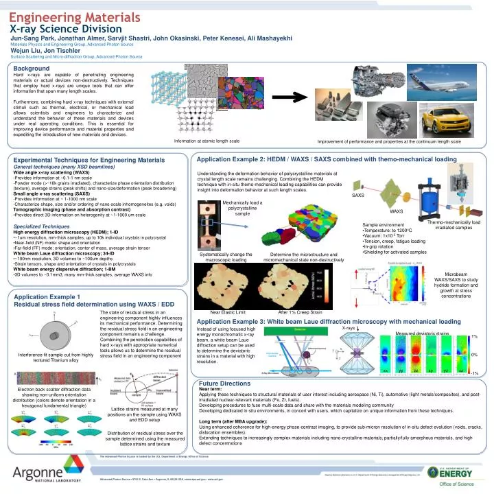
Engineering Materials X-ray Science Division Jun-Sang Park, Jonathan Almer, Sarvjit Shastri, John Okasinski, Peter Kenesei, Ali Mashayekhi Materials Physics and Engineering Group, Advanced Photon Source Wejun Liu, Jon Tischler Surface Scattering and Micro-diffraction Group, Advanced Photon Source Background Hard x-rays are capable of penetrating engineering materials or actual devices non-destructively. Techniques that employ hard x-rays are unique tools that can offer information that span many length scales. Furthermore, combining hard x-ray techniques with external stimuli such as thermal, electrical, or mechanical load allows scientists and engineers to characterize and understand the behavior of these materials and devices under real operating conditions. This is essential for improving device performance and material properties and expediting the introduction of new materials and devices. Information at atomic length scale Improvement of performance and properties at the continuum length scale Application Example 2: HEDM / WAXS / SAXS combined with themo-mechanical loading • Experimental Techniques for Engineering Materials • General techniques (many XSD beamlines) • Wide angle x-ray scattering (WAXS) • Provides information at ~0.1-1 nm scale • Powder mode (>~10k grains irradiated), characterize phase orientation distribution (texture), average strains (peak shifts) and nano-size/deformation (peak broadening) • Small angle x-ray scattering (SAXS) • Provides information at ~ 1-1000 nm scale • Characterize shape, size and/or ordering of nano-scale inhomogeneites (e.g. voids) • Tomographic imaging (phase and absorption contrast) • Provides direct 3D information on heterogenity at ~1-1000 um scale • Specialized Techniques • High energy diffraction microscopy (HEDM); 1-ID • ~1um resolution, mm-thick samples, up to 10k individual crystals in polycrystal • Near-field (NF) mode: shape and orientation • Far-field (FF) mode: orientation, center of mass, average strain tensor • White beam Laue diffraction microscopy; 34-ID • ~100nm resolution, 3D volumes to ~100um depths • Strain tensors, shape and orientation of crystals in polycrystals • White beam energy dispersive diffraction; 1-BM • 3D volumes to ~0.1mm3, many mm-thick samples, average WAXS info Understanding the deformation behavior of polycrystalline materials at crystal length scale remains challenging. Combining the HEDM technique with in-situ themo-mechanical loading capabilities can provide insight into deformation behavior at such length scales. SAXS Mechanically load a polycrystalline sample WAXS Thermo-mechanically load irradiated samples • Sample environment • Temperature: to 1200oC • Vacuum: 1x10⁻⁵ Torr • Tension, creep, fatigue loading • In-grip rotation • Shielding for activated samples Systematically change the macroscopic loading Determine the microstructure and micromechanical state non-destructively Microbeam WAXS/SAXS to study hydride formation and growth at stress concentrations Application Example 1 Residual stress field determination using WAXS / EDD Near Elastic Limit After 1% Creep Strain The state of residual stress in an engineering component highly influences its mechanical performance. Determining the residual stress field in an engineering component remains a challenge. Combining the penetration capabilities of hard x-rays with appropriate numerical tools allows us to determine the residual stress field in an engineering component Application Example 3: White beam Laue diffraction microscopy with mechanical loading X-rays Instead of using focused high energy monochromatic x-ray beam, a white beam Laue diffraction setup can be used to determine the deviatoric strains in a material with high resolution. Measured deviatoric strains 1% 0% Interference fit sample cut from highly textured Titanium alloy xx yy zz xy yz xz -1% Future Directions Near term: Applying these techniques to structural materials of user interest including aerospace (Ni, Ti), automotive (light metals/composites), and post-irradiated nuclear-relevant materials (Fe, Zr, fuels). Developing procedures to fuse multi-scale data and share with the materials modeling community Developing dedicated in-situ environments, in concert with users, which capitalize on unique information from these techniques. Electron back scatter diffraction data showing non-uniform orientation distribution (colors denote orientation in a hexagonal fundamental triangle) Lattice strains measured at many positions on the sample using WAXS and EDD setup Long term (after MBA upgrade): Using enhanced coherence for high-energy phase-contrast imaging, to provide sub-micron resolution of in-situ defect evolution (voids, cracks, dislocation ensembles). Extending techniques to increasingly complex materials including nano-crystalline materials, partially/fully amorphous materials, and high defect concentrations Distribution of residual stress over the sample determined using the measured lattice strains and texture The Advanced Photon Source is funded by the U.S. Department of Energy Office of Science Advanced Photon Source • 9700 S. Cass Ave. • Argonne, IL 60439 USA • www.aps.anl.gov • www.anl.gov