Download
1 / 20
200 likes | 354 Views
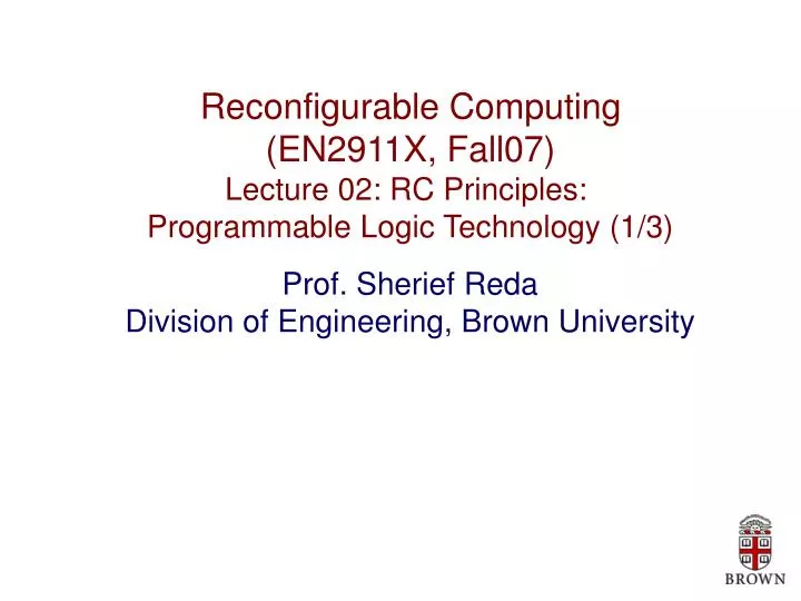
Reconfigurable Computing (EN2911X, Fall07) Lecture 02: RC Principles: Programmable Logic Technology (1/3). Prof. Sherief Reda Division of Engineering, Brown University. FPGA architecture. Programmable logic element. [Maxfield’04].

E N D
Reconfigurable Computing (EN2911X, Fall07) Lecture 02: RC Principles: Programmable Logic Technology (1/3) Prof. Sherief Reda Division of Engineering, Brown University
FPGA architecture Programmable logic element [Maxfield’04] Objective of this lecture: study organization of programmable logic blocks and interconnects
Block logic element [Rose’04] [Maxfield’04] • How is the number of bits in a K-input table? • How many Boolean functions can a K-input LUT implement? • What is the best LUT size?
F = A0A1A3 + A1A2Ā3 + Ā0 Ā1 Ā2 Example [from J. Zambreno] 4-input LUT 16 bits 3-input LUT 2-input LUT 24 bits 28 bits
Logic block clusters (logic array block LAB, configurable logic block CLB) • Assume K-input LUT in each BLE and assume N BLEs per logic cluster • The BLEs in each logic clusters are fully connected or “nearly-fully” connected • What are the best values for I, K, and N? [Betz-Rose 97]
To implement in FPGAs, designs need to be decomposed and mapped to LBs Map to a LUT in a CLB [Figure form Cong FPGA’01]
Programmable routing • Wires provide the necessary communication fabric to route the output of one computational node to the inputs of another computational node • Why routing is more crucial than logic? • Routing resources occupy a much larger area logic resources in an FPGA because circuits typically consume more routing resources for communication • Wire delay grows quadratically as a function of its length → avoid using long wires unless necessary • Technology scaling reduces device delay but increases wire delay
General routing definitions track channel CLB CLB CLB CLB segment A wire segment is a wire unbroken by programmable switches A track is a sequence of one or more wire segments in a line. The segments could be connected by switches at their ends A routing channel is a group of parallel tracks. The channel width is the number of tracks in the channel
Connection blocks: formed where CLB input or output pins connect to the routing channels Life would have been easy if only logic blocks within the same column or row need to communicate!
Segment-segment switch design for bidirectional wires track channel CLB CLB CLB CLB segment [Lemieux’04]
Switch blocks: formed wherever horizontal and vertical channels intersect Switch box Switch box size grows quadratically as a function of the number of its input wires
Bidirectional switch details [Lemieux’04, Tessier]
Segmented and hierarchical routing segmented routing hierarchical routing • Short wires accommodate local traffic • Short wires can be connected together using switch boxes to emulate longer wires • Also contain long wires to allow efficient communication without passing through switches • Routing within a “group” of logic blocks occur at the local level • Longer hierarchical wires connect different groups
Heterogeneous reconfigurable environments • Reconfigurable fabric might contain non-reconfigurable elements that interface to the logic blocks through the programmable interconnect fabric • Examples: • Embedded memory • Embedded multipliers, adders, MAC • Embedded processors
Embedded memory blocks • Costly to implement memory with configurable logic blocks → add hard chunks of RAM blocks • Position/size vary depending on the FPGA device. Size varies from few thousands (or tens of thousands) per RAM block • Each block can be used independently or combined to form larger RAM blocks • Could be single or dual-port RAMs [Maxfield’04]
Embedded multipliers and adders • Multipliers are inherently slow if implemented by connecting a large number of programmable logic blocks → add hard-wired multiplier blocks • Typically located close to the embedded RAM blocks • Some FPGA use Multiply-And-Accumulate (MAC) blocks (useful in DSP applications)
Programming the FPGA Configuration memory that determine the programmability of the logic blocks and interconnects
Programmable switch technology SRAM Anti-fuse • Switch by default is OFF; when programmed it is ON. • Advantages: • negligible delay • small area overhead • Disadvantages: • not really reconfigurable; one time programmable • SRAM bit cell stores the programmability of the device • Advantages: • can be reconfigured quickly and as repeatedly as required • no special fabrication steps • Disadvantages: • takes more area • loses charge when turned off Flash • Switch by default is ON; when programmed it is OFF. • Advantages: • programming not lost when device is turned off. • Disadvantages: • requires more manufacturing steps
Assigned readings Tuesday Sept 18 • Reconfigurable computing: A survey of systems and software. K. Compton & S. Huack (Sections 1-3) • The effect of LUT and cluster size on deep-submicron FPGA performance and density. E. Ahmed and J. Rose Thursday Sept 20 • Altera’s Stratix II vs. Xilinx’s Virtex 4 architecture comparison • Logic block organization • Interconnect organization • Non-reconfigurable components • You have to submit a 1 (or more) page summary of the paper (main ideas + critique) before midnight of the lecture day. Only use the submission form on the class website. Any summaries submitted after that time will not be looked at!
Next time Case study: Altera’s Cyclone II architecture Discussion of assigned readings


![MChem Computing and Chemistry [B14SC3]](https://cdn2.slideserve.com/4721763/mchem-computing-and-chemistry-b14sc3-dt.jpg)