Download
1 / 8
180 likes | 534 Views
The inversion layer charge Q I represents the total mobile electron charge on the surface and its expression at the source end of the channel is: Q I at x=0 =-C ox (V GS -V T0 ) and the inversion layer charge at the drain end of the channel is expressed as: Q I at x=L =-C ox (V GS -V T0 -V DS )

E N D
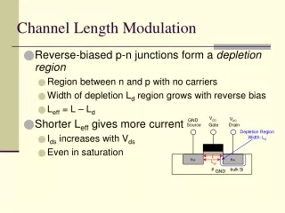
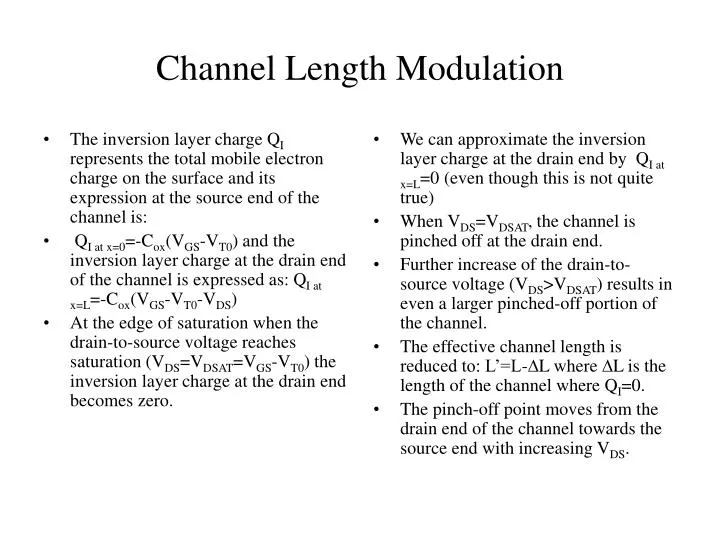
The inversion layer charge QI represents the total mobile electron charge on the surface and its expression at the source end of the channel is: QI at x=0=-Cox(VGS-VT0) and the inversion layer charge at the drain end of the channel is expressed as: QI at x=L=-Cox(VGS-VT0-VDS) At the edge of saturation when the drain-to-source voltage reaches saturation (VDS=VDSAT=VGS-VT0) the inversion layer charge at the drain end becomes zero. We can approximate the inversion layer charge at the drain end by QI at x=L=0 (even though this is not quite true) When VDS=VDSAT, the channel is pinched off at the drain end. Further increase of the drain-to-source voltage (VDS>VDSAT) results in even a larger pinched-off portion of the channel. The effective channel length is reduced to: L’=L-DL where DL is the length of the channel where QI=0. The pinch-off point moves from the drain end of the channel towards the source end with increasing VDS. Channel Length Modulation
For L’<x<L the channel voltage is Vc at x=L’=VDSAT. The electrons traveling from source to drain traverse the inverted channel segment of length L’ and then they are injected into the depletion region of length DL that separates the pinch-off point from the drain edge. The gradual channel approximation is valid in this region and is given by: IDSAT=(mnCox)/2(W/L’)[VGS-VT0]2 The effective channel length for the MOSFET operating in saturation is now L’ and the above equation accounts for the actual shortening of the channel. Shortening of the channel is also known as channel length modulation. If L’ is replaced by L in the equation we can show that the computed saturation current using L’ is greater than the new IDSAT computed using L. Channel Length Modulation
We must modify the equation for saturation current so that it reflects the dependency on VDS. Note that the saturation current will increase with increasing VDS since L’ decreases with increasing VDS. The first term of the equation accounts for the channel length modulation effect. Let 1-DL1-lVDS, with l being an empirical model parameter called the channel length modulation coefficient. Assume that lVDS<<1 then the saturation current becomes: The above equation can be used with sufficient confidence for most first order hand calculations Channel Length Modulation
So far the analysis has been on the steady state behavior of the MOS transistor. In order to examine the transient (AC) response of MOSFETs the digital circuits consisting of MOSFETs we have to determine the nature and amount of parasitic capacitances associated with the MOS transistor. On chip capacitances found on MOS circuits are in general complicated functions of the layout geometries and the manufacturing processes. Most of these capacitances are not lumped but distributed and their exact calculations would usually require complex three dimensional nonlinear charge-voltage models. A lumped representation of the capacitance can be used to analyze the dynamic transient behavior of the device. The capacitances can be classified as oxide related or junction capacitances and we will start the analysis with the oxide related capacitances. MOS Capcitances
These are Cgs and Cgd respectively. If both the source and drain regions have the same width (W), the overlap capacitance becomes: Cgs=CoxWLD and Cgd=CoxWLD. These overlap capacitances are voltage dependent. Cgs, Cgd and Cgb are voltage dependent and distributed They result from the interaction between the gate voltage and the channel charge. D Cdb Cgd G B Csb Cgs S MOS Capacitances • Masks result in some regions having overlaps, for example the gate electrode overlaps both the source and drain regions at the edges. • Two overlap capacitances arise as a result. Cgb
The gate-to-source capacitance is actually the gate-to-channel capacitance seen between the gate and the source terminals. The gate-to-drain capacitance is actually the gate-to-channel capacitance seen between the gate and the drain terminals. In Cut-off mode the surface is not inverted and there is no conducting channel linking the surface to the source and to the drain. The gate-to-source and gate-to-drain capacitances are both equal to zero (Cgs=Cgd=0). The gate-to-substrate capacitance can be approximated by: Cgb=CoxWL In linear mode the inverted channel extends across the MOSFET between the source and drain. This conducting inversion layer on the surface effectively shields the substrate from the gate electric field making it Cgb=0. MOS Oxide Capacitances
In linear mode the distributed gate-to-channel capacitance maybe viewed as being shared equally between the source and the drain leading to: Cgs=Cgd=0.5CoxWL If the MOSFET is operating in saturation mode the inversion layer on the surface does not extend to the drain, but is pinched off. The gate-to-drain capacitance in therefore zero (Cgd=0). The source is however still linked to the conducting channel. It shields the gate from the channel leading to Cgb of zero. The distributed gate-to-channel capacitance as seen between the gate and the source is approximated by: Cgs2/3CoxWL. MOSFET Oxide Capacitance