Download
1 / 1
10 likes | 160 Views
Stage II Design &Machining of Pure Molybdenum. Stage III Implementation & Temperature Profiling.

E N D
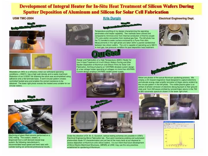
Stage II Design &Machining of Pure Molybdenum Stage III Implementation & Temperature Profiling Temperature profiling of my design characterizing the operating parameters and heater capability. Two methods were utilized and compared to minimize error from thermal conduction of thermo-couple (TC) wire and/or convection from residual gas flow. The left photo has the TC bonded to wafer surface enclosed by a Pyrex Petri dish. Measurements in the right photo are taken within a pocket sandwiched between two silicon wafers. The unit is capable of operating up to 580˚C in inert gas, low pressure condition for post deposition heat treatment. OurGoal Stage IV Deposition of Aluminum by DC Magnetron Sputtering Design and Fabrication of a High Temperature (600C) Heater for Use in Heat Treatment of 4-inch Silicon Wafers During and After Sputter Deposition of Aluminum and Silicon Films for Solar Cell Fabrication. Arching of plasma at 120VRMS dictated custom design of a low voltage heater operating at voltages no more than 40VRMS. Current design employs 24VRMS vaiable power supply. Molybdenum (MO) is a refractory metal can withstand operating conditions > 2000˚C, has a high watt density and is easily machined. Retention of our 0.0035” foil retaining the stock was accomplished using adhesive onto a flat laminate base. A semi-circular pattern creates controlled heated area and enables the correct resistance to be obtained. The lower right photo reveals the heated area suitable for our circular wafers. Below are photos of the actual Aluminum sputtering process. We employ a DC biased magnetron head designed to capture electrons and elevate energy state amplify ionization of Argon atoms evident by the circular pattern in the left photo. The visible plasma glow is an artifact of photon emission of electrons decaying back to their ground state and from EM waves emitted by ionized Argon atoms in the 700 to 800 nanometer spectrum shown in the lower right chart. Stage I Fabrication Of Heater Assembly Final Stage Testing & Assesment Machining of glass filled ceramic performed on a CNC milling. The coolant, (water), is dispensed from a self devised closed loop system. By following manufacturer’s recommended head speed and feed rates with carbide tooling we achieved professional results. Under the direction of Dr. M. G. Guvench, various testing schemes are possible in USM’s Electrical Engineering Micro-Fabrication lab. Four point resistance probing and automated photovoltaic diode I/V characterization are just two of the many tests at our disposal to assess deposition of Aluminum onto silicon wafers. It is our intent that future development of Micro Electro-Mechnical Structures, (MEMS) at USM, may use the very practices established for sputtering of Aluminum. Development of Integral Heater for In-Situ Heat Treatment of Silicon Wafers During Sputter Deposition of Aluminum and Silicon for Solar Cell Fabrication USM TMC-2004Kris DurginElectrical Engineering Dept.