Download
1 / 54
540 likes | 733 Views
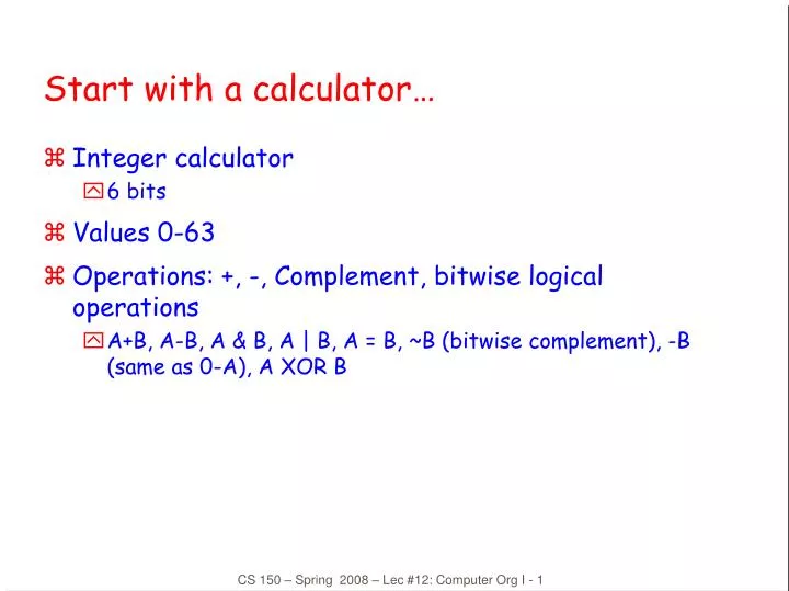
Start with a calculator… . Integer calculator 6 bits Values 0-63 Operations: +, -, Complement, bitwise logical operations A+B, A-B, A & B, A | B, A = B, ~B (bitwise complement), -B (same as 0-A), A XOR B. Calculator Layout. A. B. 6. 6. Operation. 6. C. Calculator Bit Design.

E N D
Start with a calculator… • Integer calculator • 6 bits • Values 0-63 • Operations: +, -, Complement, bitwise logical operations • A+B, A-B, A & B, A | B, A = B, ~B (bitwise complement), -B (same as 0-A), A XOR B CS 150 – Spring 2008 – Lec #12: Computer Org I - 1
Calculator Layout A B 6 6 Operation 6 C CS 150 – Spring 2008 – Lec #12: Computer Org I - 2
Calculator Bit Design • Dominated by addition Half-Adder CS 150 – Spring 2008 – Lec #12: Computer Org I - 3
Question: How do we subtract? • Tied up in: how do we represent negative numbers • Option 1: “Sign-and-Magnitude’’ • High-order bit represents sign • Low-order 5 bits represent magnitude • -7 = 10111 • Key negative: need a separate circuit for subtraction! • (How would you do it?) • Option 2: “Two’s Complement” • Take advantage of fact that 64 = 0 (in 6-bit machine) • Therefore: 64-x = -x • -7 = 64-7 = 57 = 111001 (Notice 7 = 000111) • Key: We can subtract by adding! CS 150 – Spring 2008 – Lec #12: Computer Org I - 4
Question: How do we compute two’s complement? • Positive numbers: 000001…..011111 (1 - 31) • Negative numbers: 111111….100001 (-1 - -31) • Notice: 111111 = -1 • “One’s Complement of A”: Flip each bit of A = ~A • One’s complement of 7 (000111) = 111000 • Notice: A + ~A = 111111 (-1) • XOR of each bit is 1 • AND of each bit is 0 • Therefore: -A = ~A + 1 CS 150 – Spring 2008 – Lec #12: Computer Org I - 5
Operations, Revisited • ADD, OR, AND, COMPLEMENT, EQUALITY, XOR • Negation and Subtraction implemented by manipulating inputs Per-Bit Design Carry-in to bit 0 CS 150 – Spring 2008 – Lec #12: Computer Org I - 6
Problem: Overflow • Consider 31+31 = 62 = 64-2 = -2! • Not what we want! • X+Y >= 32 (or X + Y <= -32) yield incorrect results • Numbers >= 32 or <= -32 can’t be represented • Key: detect when it happens and flag it • Exception: “Overflow” • How to detect it? • Observation I: • Can only happen when two positive or two negative numbers added together • High-order bit of operands equal • Observation II: • Happens only on an Add • Observation III: • High-Order bit of output != high-order bit of inputs CS 150 – Spring 2008 – Lec #12: Computer Org I - 7
Overflow Circuit • Also Add: • Test for negative (high-order bit is 1, “N”) • Test for zero (all bits are 0, “Z”) CS 150 – Spring 2008 – Lec #12: Computer Org I - 8
Adding multiplication • Combinational circuit is big! (see HW#1) • Roughly N^2 elements for NxN multiplication • So we do it sequentially…just use the algorithm we all learned in school • Partial result = 0, multiplier = A, multiplicand = B • For I = 1 to Nbits-1 • if lsb of multiplier is 1, result = result + multiplicand • Multiplicand = multiplicand << 1 • Multiplier = multiplier >> 1 • What about sign? • Simple algorithm (not optimal!) • S = sign(A x B) • C = |A|x|B| • if (S) result = -C else result = C CS 150 – Spring 2008 – Lec #12: Computer Org I - 9
What do we need? • Minor: • Shifter (too easy to spend class time on!) • Test lsb for 1/0 (just run an extra wire from low-order input to ALU) • Major: • Place to store partial results • Place to store sign of result • Actions dependent on values • Program for multiplication algorithm • These are easy, but change the character of the device! CS 150 – Spring 2008 – Lec #12: Computer Org I - 10
Multiplying Calculator Layout Registers Control FSM A B 6 6 Operation 6 C CS 150 – Spring 2008 – Lec #12: Computer Org I - 11
Control FSM: Timing is Key • Basically the same program we saw before, BUT • Need to keep track of timing! • Compute sign of result • Load multiplier with |A| • Load multiplicand with |B| • Load partial result with 0 • If lsb of multiplier is 1 • Add multiplicand to partial result • Shift multiplier right • Shift multiplicand left • Negate result if needed CS 150 – Spring 2008 – Lec #12: Computer Org I - 12
By This time, we’re getting close to something else… CS 150 – Spring 2008 – Lec #12: Computer Org I - 13
What do we we have • Control program in FSM that sequences instructions • Storage that are loaded in response to data conditions • Actions taken, or not, in response to conditions • This is better known as a computer • All we have to add is memory CS 150 – Spring 2008 – Lec #12: Computer Org I - 14
Computer design as an application of digital logic design procedures Computer = processing unit + memory system Processing unit = control + datapath Control = finite state machine Inputs = machine instruction, datapath conditions Outputs = register transfer control signals, ALU operation codes Instruction interpretation = instruction fetch, decode, execute Datapath = functional units + registers Functional units = ALU, multipliers, dividers, etc. Registers = program counter, shifters, storage registers Computer Organization CS 150 – Spring 2008 – Lec #12: Computer Org I - 15
+ Tri-State Buffers • 0, 1, Z (high impedance state) Basic Inverter in out in OE out + OE if OE then Out = In else “disconnected” out in Inverting Buffer CS 150 – Spring 2008 – Lec #12: Computer Org I - 16
Tri-States vs. Mux A B A B Sel0 D E C 0 1 2:1 Mux Sel Sel 0 1 Sel1 Buffer circuits simple! Scales nicely for high fan-in and wide bit widths! Scales poorly for high fan-inor wide bit widths CS 150 – Spring 2008 – Lec #12: Computer Org I - 17
Register Transfer C A Sel 0; Ld 1 C B Sel 1; Ld 1 A B Sel0 D E C Sel 0 1 Sel1 Bus Clk Sel Ld Ld C Clk A on Bus B on Bus Ld C from Bus ? CS 150 – Spring 2008 – Lec #12: Computer Org I - 18
+ + Bad! Short circuit! Low resistance path fromVdd to Gnd Open Collector Concept Resistive Pull-up “1” Default is high Must actively drive it low “1” “0” “0” Wired AND Configuration: If any attached device wants wire to be “0”, it wins If all attached devices wantwire to be “1”, it is CS 150 – Spring 2008 – Lec #12: Computer Org I - 19
address Memory System Processor read/write data central processing unit (CPU) control signals Control Data Path data conditions instruction unit– instruction fetch and interpretation FSM execution unit– functional units and registers Structure of a Computer • Block diagram view CS 150 – Spring 2008 – Lec #12: Computer Org I - 20
OE Q7 Q6 Q5 Q4 Q3 Q2 Q1 Q0 LD D7 D6 D5 D4 D3 D2 D1 D0 CLK Registers • Selectively loaded – EN or LD input • Output enable – OE input • Multiple registers – group 4 or 8 in parallel OE asserted causes FF state to be connected to output pins; otherwise they are left unconnected (high impedance) LD asserted during a lo-to-hi clock transition loads new data into FFs CS 150 – Spring 2008 – Lec #12: Computer Org I - 21
MUX MUX MUX MUX rt rs rd R4 rd rs R4 rt R4 rs rt rd MUX BUS Register Transfer • Point-to-point connection • Dedicated wires • Muxes on inputs ofeach register • Common input from multiplexer • Load enablesfor each register • Control signalsfor multiplexer • Common bus with output enables • Output enables and loadenables for each register CS 150 – Spring 2008 – Lec #12: Computer Org I - 22
RE RB RA WE WB WA D3 D2 D1 D0 Q3 Q2 Q1 Q0 Register Files • Collections of registers in one package • Two-dimensional array of FFs • Address used as index to a particular word • Separate read and write addresses so can do both at same time • 4 by 4 register file • 16 D-FFs • Organized as four words of four bits each • Write-enable (load) • Read-enable (output enable) CS 150 – Spring 2008 – Lec #12: Computer Org I - 23
RD WR A9 A8 A7 A6 A5 A4 A3 A2 A2 A1 A0 IO3 IO2 IO1 IO0 Memories • Larger Collections of Storage Elements • Implemented not as FFs but as much more efficient latches • High-density memories use 1-5 switches (transitors) per bit • Static RAM – 1024 words each 4 bits wide • Once written, memory holds forever (not true for denser dynamic RAM) • Address lines to select word (10 lines for 1024 words) • Read enable • Same as output enable • Often called chip select • Permits connection of manychips into larger array • Write enable (same as load enable) • Bi-directional data lines • output when reading, input when writing CS 150 – Spring 2008 – Lec #12: Computer Org I - 24
Instruction Sequencing • Example – an instruction to add the contents of two registers (Rx and Ry) and place result in a third register (Rz) • Step 1: Get the ADD instruction from memory into an instruction register • Step 2: Decode instruction • Instruction in IR has the code of an ADD instruction • Register indices used to generate output enables for registers Rx and Ry • Register index used to generate load signal for register Rz • Step 3: Execute instruction • Enable Rx and Ry output and direct to ALU • Setup ALU to perform ADD operation • Direct result to Rz so that it can be loaded into register CS 150 – Spring 2008 – Lec #12: Computer Org I - 25
Instruction Types • Data Manipulation • Add, subtract • Increment, decrement • Multiply • Shift, rotate • Immediate operands • Data Staging • Load/store data to/from memory • Register-to-register move • Control • Conditional/unconditional branches in program flow • Subroutine call and return CS 150 – Spring 2008 – Lec #12: Computer Org I - 26
Elements of the Control Unit (aka Instruction Unit) • Standard FSM Elements • State register • Next-state logic • Output logic (datapath/control signaling) • Moore or synchronous Mealy machine to avoid loops unbroken by FF • Plus Additional ”Control" Registers • Instruction register (IR) • Program counter (PC) • Inputs/Outputs • Outputs control elements of data path • Inputs from data path used to alter flow of program (test if zero) CS 150 – Spring 2008 – Lec #12: Computer Org I - 27
Instruction Execution Reset • Control State Diagram (for each diagram) • Reset • Fetch instruction • Decode • Execute • Instructions partitioned into three classes • Branch • Load/store • Register-to-register • Different sequencethrough diagram for each instruction type Init InitializeMachine FetchInstr. Load/Store XEQInstr. Branch Register-to-Register Branch Taken BranchNot Taken Incr.PC CS 150 – Spring 2008 – Lec #12: Computer Org I - 28
Cin Ain FA Sum Bin Cout Ain Sum HA Bin Cout HA Cin Data Path (Hierarchy) • Arithmetic circuits constructed in hierarchical and iterative fashion • Each bit in datapath is functionally identical • 4-bit, 8-bit, 16-bit, 32-bit datapaths CS 150 – Spring 2008 – Lec #12: Computer Org I - 29
A B 16 16 Operation 16 N S Z Data Path (ALU) • ALU Block Diagram • Input: data and operation to perform • Output: result of operation and status information CS 150 – Spring 2008 – Lec #12: Computer Org I - 30
16 REG AC 16 16 OP N 16 Z Data Path (ALU + Registers) • Accumulator • Special register • One of the inputs to ALU • Output of ALU stored back in accumulator • One-address instructions • Operation and address of one operand • Other operand and destinationis accumulator register • AC <– AC op Mem[addr] • ”Single address instructions”(AC implicit operand) • Multiple registers • Part of instruction usedto choose register operands CS 150 – Spring 2008 – Lec #12: Computer Org I - 31
CO CO ALU CI ALU ALU CI AC AC AC rt R0 rs rt rd rd rs rt rd R0 rs R0 frommemory frommemory frommemory Data Path (Bit-slice) • Bit-slice concept: iterate to build n-bit wide datapaths 1 bit wide 2 bits wide CS 150 – Spring 2008 – Lec #12: Computer Org I - 32
Instruction Path • Program Counter • Keeps track of program execution • Address of next instruction to read from memory • May have auto-increment feature or use ALU • Instruction Register • Current instruction • Includes ALU operation and address of operand • Also holds target of jump instruction • Immediate operands • Relationship to Data Path • PC may be incremented through ALU • Contents of IR may also be required as input to ALU CS 150 – Spring 2008 – Lec #12: Computer Org I - 33
Data Path (Memory Interface) • Memory • Separate data and instruction memory (Harvard architecture) • Two address busses, two data busses • Single combined memory (Princeton architecture) • Single address bus, single data bus • Separate memory • ALU output goes to data memory input • Register input from data memory output • Data memory address from instruction register • Instruction register from instruction memory output • Instruction memory address from program counter • Single memory • Address from PC or IR • Memory output to instruction and data registers • Memory input from ALU output CS 150 – Spring 2008 – Lec #12: Computer Org I - 34
Block Diagram of Processor • Register Transfer View of Princeton Architecture • Which register outputs are connected to which register inputs • Arrows represent data-flow, other are control signals from control FSM • MAR may be a simple multiplexerrather than separate register • MBR is split in two(REG and IR) • Load control for each register load path 16 REG AC rd wr storepath 16 16 data Data Memory (16-bit words) OP addr N 16 Z ControlFSM MAR 16 IR PC 16 16 OP 16 CS 150 – Spring 2008 – Lec #12: Computer Org I - 35
Block Diagram of Processor • Register transfer view of Harvard architecture • Which register outputs are connected to which register inputs • Arrows represent data-flow, other are control signals from control FSM • Two MARs (PC and IR) • Two MBRs (REG and IR) • Load control for each register load path 16 REG AC rd wr storepath 16 16 data Data Memory (16-bit words) OP addr N 16 Z ControlFSM 16 IR PC data Inst Memory (8-bit words) 16 16 OP addr 16 CS 150 – Spring 2008 – Lec #12: Computer Org I - 36
A Simplified Processor Data-path and Memory memory has only 255 wordswith a display on the last one • Princeton architecture • Register file • Instruction register • PC incremented through ALU • Modeled afterMIPS rt000(used in 61Ctextbook byPatterson &Hennessy) • Really a 32 bitmachine • We’ll do a 16 bitversion CS 150 – Spring 2008 – Lec #12: Computer Org I - 37
Processor Control • Synchronous Mealy machine • Multiple cycles per instruction CS 150 – Spring 2008 – Lec #12: Computer Org I - 38
Processor Instructions • Three principal types (16 bits in each instruction) type op rs rt rd funct R(egister) 3 3 3 3 4 I(mmediate) 3 3 3 7 J(ump) 3 13 • Some of the instructionsadd 0 rs rt rd 0 rd = rs + rt sub 0 rs rt rd 1 rd = rs - rt and 0 rs rt rd 2 rd = rs & rt or 0 rs rt rd 3 rd = rs | rt slt 0 rs rt rd 4 rd = (rs < rt) lw 1 rs rt offset rt = mem[rs + offset] sw 2 rs rt offset mem[rs + offset] = rt beq 3 rs rt offset pc = pc + offset, if (rs == rt) addi 4 rs rt offset rt = rs + offset j 5 target address pc = target address halt 7 - stop execution until reset R I J CS 150 – Spring 2008 – Lec #12: Computer Org I - 39
Tracing an Instruction's Execution • Instruction: r3 = r1 + r2R 0 rs=r1 rt=r2 rd=r3 funct=0 • 1. Instruction fetch • Move instruction address from PC to memory address bus • Assert memory read • Move data from memory data bus into IR • Configure ALU to add 1 to PC • Configure PC to store new value from ALUout • 2. Instruction decode • Op-code bits of IR are input to control FSM • Rest of IR bits encode the operand addresses (rs and rt) • These go to register file CS 150 – Spring 2008 – Lec #12: Computer Org I - 40
Tracing an Instruction's Execution (cont’d) • Instruction: r3 = r1 + r2R 0 rs=r1 rt=r2 rd=r3 funct=0 • 3. Instruction execute • Set up ALU inputs • Configure ALU to perform ADD operation • Configure register file to store ALU result (rd) CS 150 – Spring 2008 – Lec #12: Computer Org I - 41
Tracing an Instruction's Execution (cont’d) • Step 1 CS 150 – Spring 2008 – Lec #12: Computer Org I - 42
to controller Tracing an Instruction's Execution (cont’d) • Step 2 CS 150 – Spring 2008 – Lec #12: Computer Org I - 43
Tracing an Instruction's Execution (cont’d) • Step 3 CS 150 – Spring 2008 – Lec #12: Computer Org I - 44
Register-Transfer-Level Description • Control • Transfer data btwn registers by asserting appropriate control signals • Register transfer notation: work from register to register • Instruction fetch: mabus PC; – move PC to memory address bus (PCmaEN, ALUmaEN) memory read; – assert memory read signal (mr, RegBmdEN) IR memory; – load IR from memory data bus (IRld) op add – send PC into A input, 1 into B input, add (srcA, srcB0, scrB1, op) PC ALUout – load result of incrementing in ALU into PC (PCld, PCsel) • Instruction decode: IR to controller values of A and B read from register file (rs, rt) • Instruction execution: op add – send regA into A input, regB into B input, add (srcA, srcB0, scrB1, op) rd ALUout – store result of add into destination register (regWrite, wrDataSel, wrRegSel) CS 150 – Spring 2008 – Lec #12: Computer Org I - 45
Register-Transfer-Level Description (cont’d) • How many states are needed to accomplish these transfers? • Data dependencies (where do values that are needed come from?) • Resource conflicts (ALU, busses, etc.) • In our case, it takes three cycles • One for each step • All operation within a cycle occur between rising edges of the clock • How do we set all of the control signals to be output by the state machine? • Depends on the type of machine (Mealy, Moore, synchronous Mealy) CS 150 – Spring 2008 – Lec #12: Computer Org I - 46
decode execute fetch step 1 step 2 step 3 IR mem[PC]; PC PC + 1; A rs B rt rd A + B to configure the data-path to do this here, when do we set the control signals? Review of FSM Timing CS 150 – Spring 2008 – Lec #12: Computer Org I - 47
FSM Controller for CPU (skeletal Moore FSM) • First pass at deriving the state diagram (Moore Machine) • These will be further refined into sub-states reset instructionfetch instructiondecode SW J ADD instructionexecution LW CS 150 – Spring 2008 – Lec #12: Computer Org I - 48
FSM Controller for CPU (reset and instruction fetch) • Assume Moore Machine • Outputs associated with states rather than arcs • Reset state and instruction fetch sequence • On reset (go to Fetch state) • Start fetching instructions • PC will set itself to zero mabus PC; memory read; IR memory data bus; PC PC + 1; reset instructionfetch Fetch CS 150 – Spring 2008 – Lec #12: Computer Org I - 49
FSM Controller for CPU (decode) • Operation Decode State • Next state branch based on operation code in instruction • Read two operands out of register file • What if the instruction doesn’t have two operands? instructiondecode Decode branch based on value ofInst[15:13] and Inst[3:0] add CS 150 – Spring 2008 – Lec #12: Computer Org I - 50