Download
1 / 84
840 likes | 1.26k Views
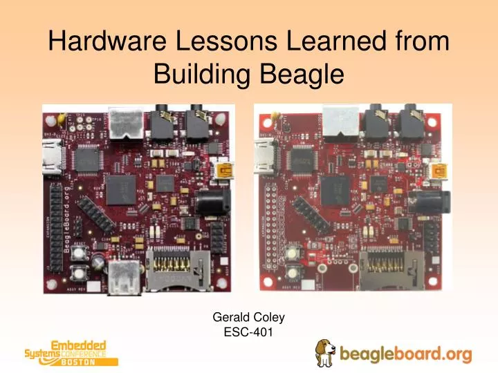
Hardware Lessons Learned from Building Beagle Gerald Coley ESC-401 Topics Covered What’s in a name? Specification Schematic PCB Layout Assembly Testing Support Implementing Lessons Learned Questions and discussion The Name: Where did we get the name BeagleBoard?

E N D
Hardware Lessons Learned from Building Beagle Gerald Coley ESC-401
Topics Covered • What’s in a name? • Specification • Schematic • PCB Layout • Assembly • Testing • Support • Implementing Lessons Learned • Questions and discussion
How did we arrive at BeagleBoard? • Every project needs a name • Named for my dog. • Just “temporary” • We will fix it later • Well, It Stuck • A Beagle is: • Like Tux, non threatening • Curious • Loyal • Fun • And gives back as much as it receives • Lesson Learned…If you name it, it will stick!
So, we need an acronym • Bring your own peripherals • Entry-level • ARM Cortex-A8 • Graphics & DSP • Linux and open source • Environment for SW innovators
The Goals • Get OMAP3530 into people’s hands • Low Cost <$150 • Under the spousal radar • Reach as many people as we can • Small Size • Keeps the cost down • “Cool” Factor • Internally focused • Cortex-A8 + NEON • DSP • 3D Graphics • Accelerators
First Pass Features • OMAP3530 Processor • 3.5” LCD • VGA/QVGA • Touch screen • S-Video • Keypad • 2 Serial Ports • SD/MMC • Ethernet • Camera • 128MB DDR • 128MB NAND • USB • Host • OTG • USB/DC Power • Stereo In/Out • Battery w/Charger • Full Expansion Bus COST: $1500 Size: 5” x 8” Something has to go!!
Bring Your Own • Not everyone needs everything • Everything is needed • Bring your Own • User adds only what they need • They don’t have to pay for what they already have • Allows for maximum exposure to HW • More than just one component supplier
Final Pass Features Standard on Beagle Bring your own • OMAP3530 • 3.5” LCD.-VGA/QVGA • Touch screen USB Touch Screen • DVI-D VGA, SVGA, XGA • S-Video • Keypad • 1 button USB Keyboard & Mouse • 2 Serial Ports • 1 Port USB &Expansion • SD/MMC 6 in 1 Slot • Ethernet • USB Dongle & WiFI • Camera • USB Camera • 128MB DDR • 128MB NAND • USB Host OTG • USB/DC Power • Stereo In/Out • Battery w/Charger • USB Battery Adapter • Size 5” x 8” 3” x 3” • Full Expansion Bus • Standard buses COST: $149 Just meat and potatoes, but still room for dessert!!
Play It Safe • Leverage everything we can • Used OMAP35xx EVM as base • Maintain compatibility with other platforms • Common hookup • Subset used the same • Keep the component count low • Use what is proven to work • Leave off what is not needed
Leveraged Advantages • OMAP35xx Processor Symbol/Design verified • TWL4030/TPS65950 Symbol/Design verified • Removed a lot of features here • SD/MMC Verified • DVI-D verified • UART Verified • Lowered the overall risk
Rules We Used PCB Design PCB FAB PCB ASSEMBLY TI Memory Vendors Failure to include the fab and assembly team members can prove costly since choices made early in the design will adversely impact the final cost of the assembled board
The Challenges • OMAP35xx Package • .4mm Pitch • Routing • TPS65950(TWL4030) • .4mm pitch PMIC • POP Implications • Limited area for connectors • Location driven and not layout driven
What Exactly Is POP? Memory OMAP
Fixed Location of Connectors • Routing complicated by locations • Connector not always on the best side • We tried to make this as easy as possible • Not the best locations for routing • The DVI-D was the longest route • We need to keep the layer count down • Our goal was to stick with 6 layers
via BGA Good Trace should never be larger than pad Better Don’t gang BGA pads with ground plane Best Recommended Trace and Via Connections Poor Better Watch for solder traps
Blind and Buried Vias • Definitions and Terminology • • Through hole via has access to both external layers • • Buried via provides connection within inner layers • Blind via does not pass through the entire board
Via-in-Pad • Places the via directly in the BGA pad • Greatly improves board routing • Has special requirements for manufacturability • Given a 10mil BGA pad • Use a 4mil microvia • Laser drilled • Via must be filled or capped to minimize void formation • Via-fill Material • Check with board fabricator for their preferences • Fill material can be conductive or non-conductive • Via fill material’s particle size must be <1mil for complete penetration You must validate your board fabricator’s capability to reliably build with this class of technology
.4mm Pitch • No routing between pads • Use top layer routing on outside pads • Use vias-in-pad wherever needed
Soldermask • Exposed pad should be the same size as the pad on the mounted device • Need to make the pad larger to add stability • Calls for soldermask defined pads
Surface Finish The PCB surface finish provides a coating over the outer layer copper that prevents oxidation and provides an electrically conductive surface. • Organic Solderability Preservative (OSP) Thin layer of organic material to prevent copper oxidation. It is removed by the assembly flux. Does not tolerate multiple heat cycles. • Immersion Tin (ImSn) Thin layer of tin directly on top of the copper surface. Produces an extremely flat surface for mounting of surface mount components. Downside is the possible formation of Tin whiskers. • Immersion Silver (ImAg) Thin layer of silver directly on top of the copper surface. Produces a very flat surface. Compatible with no-clean assembly processes. Maintains high solderability after multiple heat cycles. Downside is that the plating will tarnish over time. • Electroless Nickel Immersion Gold (ENIG) Commonly used finish that is nice and flat for fine-pitch devices. Not easily reworked and more expensive. • Hot-air solder leveling (HASL) Immersing the PCB in solder. It is inexpensive and widely available, but it is not flat and therefore does not work well with fine-pitch devices
TFP410 OMAP3 Triton-2 Final BeagleBoard Design
OMAP3530 BGA Footprint Pad Type Solder Mask Defined Pad Pitch A 400um Pad Opening B 254um (10mils) Pad Dia C 280um (11mils) Mask Web D 150um
Via-In-Pad Topology • Stacked Microvia-In-Pad • Pad 11mils copper (10mil SMD) • Top-Layer2 stacked with Layer2-Layer-3 • Top-Layer2 • Laser Drill 6mil (0.152mm) • Solder-mask defined pads • Non-conductive epoxy via plugs, plated over and planarized BeagleBoard does not use buried vias OMAP3 Top Soldermask Top Signal Blind 1-2 Blind/Stacked 1-3 Lyr2-GND Lyr3-SIG Lyr4-SIG Lyr5-PWR Bottom Signal Bottom Soldermask
Standard Vias • Thru-hole via from top to bottom • 18mil radius pad • 8 mil drilled hole • Plugged, plated and planarized • Must be level • No dimples Top Lyr2-GND Lyr3-SIG Lyr4-SIG Lyr5-PWR Bottom Not To Scale
Top Layer-Signal (Area under OMAP3 Chip) Via 1-6 V-I-P BGA PAD 3mil trace 10mil trace
Bypass Capacitor Location and Solder Pads Via 1-6 Component Pad • Min trace width 3 mils Bottom Layer Bypass Capacitor Locations Capacitor Spec Type: Ceramic X7R Size: 402 Value: 0.1uF
PCB Fabrication Concerns • High Board cost • Because they can charge more • Unknown = $$$$$ • Does not necessarily mean the production $$ will be high • Unfamiliar with fine pitch • Soldermask registration critical
POP Assembly Concerns • POP was the number one concern • Nitrogen and air were the two options • What should we do? • Picked the one that was the most applicable to as many assembly houses as possible….Air • POP soldering in air • Air #1 • Air #2
Mounting .4mm Parts • No real concerns • Equipment can handle it • Warping of the processor due to POP was a possibility • Saw no reason to be concerned • There could be an issue with shorts if soldermask not correct • We were comfortable
Pick and Place Machine My DATA (MY9) D-014-1486 F30
Reflow Oven Heller EXL
X-Ray Machine Glenbrook Technologies RTX-113
POP Mounting Configurations • Method A • POP onto OMAP3 first reflow • Back side Second reflow • Top side third w/POP+OMAP3530 reflow • Method B • Mount back side reflow • Mount top side with OMAP3530 reflow • Mount Memory w/ Pick & Place reflow • Method C • Mount backside reflow • Mount topside with OMAP3530 and POP reflow
Method A Process Hand Mount TopGEL POP Mount w/SMT OMAP3 OMAP3 Paste SMT Reflow Reflow Paste Top side of board Bottom side of board Hand Assembly
Method B Process Paste Paste SMT Reflow SMT Reflow Top side of board Bottom side of board ApplyGel POP Memory SMT Reflow Hand Assembly
Method C Process Dipping Arm is used to apply paste POP Memory POP Memory Paste Paste SMT Reflow Reflow SMT Top side of board Bottom side of board Hand Assembly
POP Mounting Analysis • Method A • No real issues seen • We abandoned it when we ran into issues • Issues were not related to this process • Method B • Final method adopted • Have had excellent results • Method C • Dipping Arm…POP Memory dipped into GEL • Have a lot of high volume customers doing this • Did not try as we had no dipping arm
Panelization • Method A • 4 boards per panel • Used it on the first runs • Had concerns about warping across the scoring that could cause solder shorts • Nothing ever proven that this was an issue • Method B • One board per panel • Method chosen
Other Parameters • Stencil thickness • .4mils • Solder Paste • AMTECH LF -4300 Lead Free • Chemistry Sn96.5/Ag3.0/Cu.5 • Tacky paste flux (memory) • Amtech Tacky Solder Flux
Peak 250 200 Temperature - Degrees C 150 100 50 Preheating stage Cooldown Reflow Reflow Profile Diagram Time
Issues on 1st Run • Solder Shorts under the processor • Always a power rail • 10% Yields • Could it be related to….? • POP Package • Profile • PCB • Parts • Solder