Download
1 / 1
10 likes | 188 Views
Selective CdTe Single Crystal Deposition with High-Areal Density. Daniel C. Ralph, Cornell University, ECCS - 0335765.

E N D
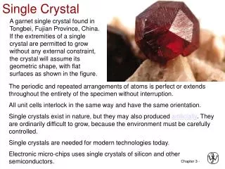
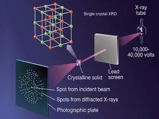
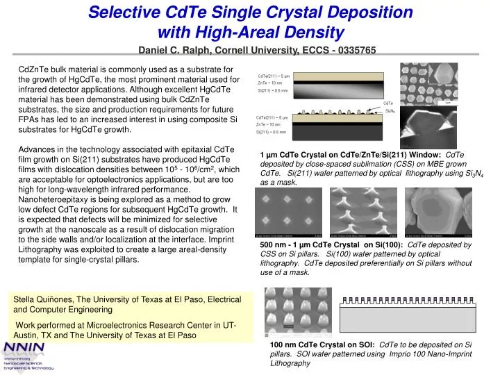
Selective CdTe Single Crystal Deposition with High-Areal Density Daniel C. Ralph, Cornell University, ECCS - 0335765 CdZnTe bulk material is commonly used as a substrate for the growth of HgCdTe, the most prominent material used for infrared detector applications. Although excellent HgCdTe material has been demonstrated using bulk CdZnTe substrates, the size and production requirements for future FPAs has led to an increased interest in using composite Si substrates for HgCdTe growth. Advances in the technology associated with epitaxial CdTe film growth on Si(211) substrates have produced HgCdTe films with dislocation densities between 105 - 106/cm2, which are acceptable for optoelectronics applications, but are too high for long-wavelength infrared performance. Nanoheteroepitaxy is being explored as a method to grow low defect CdTe regions for subsequent HgCdTe growth. It is expected that defects will be minimized for selective growth at the nanoscale as a result of dislocation migration to the side walls and/or localization at the interface. Imprint Lithography was exploited to create a large areal-density template for single-crystal pillars. 1 µm CdTe Crystal on CdTe/ZnTe/Si(211) Window: CdTe deposited by close-spaced sublimation (CSS) on MBE grown CdTe. Si(211) wafer patterned by optical lithography using Si3N4 as a mask. 500 nm - 1 µm CdTe Crystal on Si(100): CdTe deposited by CSS on Si pillars. Si(100) wafer patterned by optical lithography. CdTe deposited preferentially on Si pillars without use of a mask. Stella Quiñones, The University of Texas at El Paso, Electrical and Computer Engineering Work performed at Microelectronics Research Center in UT-Austin, TX and The University of Texas at El Paso 100 nm CdTe Crystal on SOI: CdTe to be deposited on Si pillars. SOI wafer patterned using Imprio 100 Nano-Imprint Lithography