Download
1 / 21
210 likes | 212 Views
This article discusses the R&D phase of the NED conductor development and production at SMI, including steps taken, heat treatment optimization studies, and the final production and characterization of the conductor.

E N D
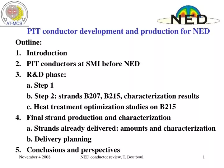
PIT conductor development and production for NED • Outline: • Introduction • PIT conductors at SMI before NED • R&D phase: • a. Step 1 • b. Step 2: strands B207, B215, characterization results • c. Heat treatment optimization studies on B215 • Final strand production and characterization • a. Strands already delivered: amounts and characterization • b. Delivery planning • 5. Conclusions and perspectives NED conductor review, T. Boutboul
Introduction • Following call for tender in Summer 2004, ShapeMetal Innovation (SMI, Enschede, The Netherlands) awarded a NED contract (300 k€) for Powder-In-Tube (PIT) conductor. • PIT technique developed by ECN (since 1975) and purchased by SMI in 1992. • PIT technology acquired by EAS (Germany, now Bruker EAS) in December 2006 • PIT: NbSn2 powder (possibly enriched with pure Sn) compacted and inserted into a Nb-X/Cu tube. After tube drawing to smaller diameter, stacked into Cu tube with a Cu core for final cold drawing. NED conductor review, T. Boutboul
PIT conductor situation at SMI before NED Before NED, SMI “state of the art” strand: B179 • Jc ~ 2280 A/mm2 @ 12 T. • 192 filaments, deff ~ 54 µm but for strand diameter of 1 mm (~70 µm at 1.25 mm vs < 50 µm). • For D=1.25 mm, needed morefilaments. • Strand very sensitive to deformation. For NED (Step 1), SMI worked on improving Jc (powder, barrier, HT) NED conductor review, T. Boutboul
R&D phase: Step 1 During Step 1, SMI developed two strands (1 mm in diameter instead of 1.25 mm, ~ 50 µm filaments): B201 and B205 (~ 320 m for both). B201: 192 filaments, to improve Jc SMI added free Sn to NbSn2powder but, during HT, Sn leaks!! B201, SEM B201, Optical B201, no heat treatment B205: less Sn-enriched powder used than B201 but Sn leaks as well… NED conductor review, T. Boutboul
R&D phase: Step 1 (end) • Upon CERN request, B201 strand design incorporated more copperbetween the filaments (tubes) than B179 for an improved mechanical behavior following cabling deformation: Flat rolling deformation 25 % def. B179 B201 • Two billets with Ta barrier tried for full reaction but very serious workability troubles… • HT: 84 h (instead of 64 h) @ 675 oC on B179: Jc ~ 2410 A/mm2, 12 T NED conductor review, T. Boutboul
R&D phase (Step 2): B207 • For the Step 2, SMI produced a strand, B207 (~ 300 m long), including 288 filaments, nominal NED diameter (1.25 mm) but Cu/non-Cu = 0.96 (instead of 1.25) due to bad die selection at drawing beginning. • Even more copper inserted between filaments than B201 strand to further improve mechanical behavior. Powder composition as B179. • However: Jc = 2077 A/mm2 (12 T), 1118 A/mm2 (15 T), i.e. ~ 13 %lower than B179: disappointing. RRR = 250 (virgin), 40-80 (def.). Low Jc due to a mistake during powder preparation. NED conductor review, T. Boutboul
R&D phase (Step 2): B215 • B215 strand fabricated (summer 2006) according to B207 design. • 950 m produced in a lone length. • 288 filaments (~ 50 µm) fulfilling NED specification. • Adequate Cu/non-Cu (~ 1.22) and Strand diameter (1.257 mm). B215 cross-section (no heat treatment) NED conductor review, T. Boutboul
B215 strand characterization (standard HT) • Critical current measurements done at CERN, INFN/Milan and Twente University with the heat treatment recommended by SMI (84 h @ 675 oC). • Max. measuredJc ~ 2500 A/mm2 in non-copper part, Ic=1397 A (Twente), 12 T and 4.2 K. • Combination of high Ic (12 T) and fine filament size (~ 50 µm): world record!! • Ic=756 A @ 15 T, 4.2 K (only 8 % below spec.), Jc=1350 A/mm2(Geneva). NED conductor review, T. Boutboul
B215 strand characterization (standard HT) • Acceptable: RRR ~ 70-80 (virgin samples). • Magnetization measurements (Frascati) on VSM instrument: few flux jumps! NED conductor review, T. Boutboul
0.20 µm 0.21 µm 0.23 µm 0.22 µm HT optimization studies on B215: motivation • In PIT reacted strands: A15 phase composed of coarse grains (1-2 µm, ~ 30 %) and fine grains (~ 200 nm). Jccontribution of coarse grains negligible. • The idea: try to improve Ic and RRR by reaction temperaturedecrease in order to (tentatively): • To reducefine Nb3Sn grain size • To reduce coarse grain area (possible?) B215 sample, 84 h @ 675 oC NED conductor review, T. Boutboul
HT optimization studies on B215: method • Due to limited amounts of available B215 strand and to limited reaction oven resources , a systematic optimization study with broad scanning of treatment temperature and duration not possible. • Instead, a kind of “trial and error” method used: a specific HT schedule is selected, then Ic, RRR measured, cross-section examined at microscope to evaluate the extent of the reacted area. According to these results, the next schedule is chosen… • Various temperatures and durations already tried with the same temperature ramp of 50 oC/hour: • 660 oC: 84 h • 650 oC: 84 h, 120 h • 625 oC: 200 h, 260 h, 320 h and 400 h NED conductor review, T. Boutboul
Prominent results 120 h @ 650 oC • Ic measurements performed at CERN and Twente. Consistent Icdata measured with maximal value of 1410 A (12 T, 4.2 K), corresponding to Jc ~ 2520 A/mm2, ~ 1 % larger than 84 h @ 675 oC. • Although slight increase not significant, measurements more reproducible (Icscatter of less than 3 % versus ~6 % for standard HT). • Measurements at Geneva: 1 % as well at 15 T and 4.2 K, Bc2K~25.6 T. • From RRR point of view, 120 h @ 650 oC appears to be more favorable than 84 h @ 675 oC. Indeed, RRR values, generally larger than 100 (max. 143) for 120 h @ 650 oC as compared to values not exceeding 80 (standard HT schedule). NED conductor review, T. Boutboul
320 h @ 625 oC After treatments at 650 oC, decided to try 625 oC. As preliminary test, B215 sample treated 61 h @ 620 oC to check reaction feasibility at such low temperature. • Good news: thin A15 layer already reacted (dark grey). • Bad news: large area of Nb6Sn5 (white layer close to core) also present, to be converted to Nb3Sn coarse grains (at least 25 % of reacted Nb3Sn phase). Courtesy of G. Arnau and C. Scheuerlein NED conductor review, T. Boutboul
320 h @ 625 oC (continuation) • After two trials at 625 oC (200 and 260 hours), 2 samples were treated 320 h @ 625 oC at CERN, 2 additional samples reacted at Twente. • Icdata consistently measured at CERN and Nijmegen in the range: Ic = 1494-1539 A @ 12 T, 4.22 K, corresponding to Jc ~ 2700 A/mm2, + 10 % as compared to standard HT. • 15 T, 4.222 K: Ic > 818 A (NED spec.), Jc ~ 1500 A/mm2 • New record!!B215 strand completely fulfilling NED specification. • RRR data impressive as well since RRR ~ 220 for virgin strands!! Better for stability. • Last treatment: 400 h @ 625 oC but no Ic gain and lower RRR (~ 120) NED conductor review, T. Boutboul
320 h @ 625 oC (continuation) Bc2K = 26.3 T (vs 25.6 T) Stringent NED specification fulfilled!! NED conductor review, T. Boutboul
Specific heat measurements on B215 (University of Geneva) Courtesy of C. Senatore and R. Flukiger (Geneva Univ.) NED conductor review, T. Boutboul
SEM examinations on B215 polished and fractured samples Sample with optimized HT: less reacted Nb3Sn but with higher quality: higher Sn content, Bc2K, Tc and smaller grain size (160 nm vs 180 nm) NED conductor review, T. Boutboul
Final strand production and characterization (1) • Following successful R&D, EAS/SMI was awarded the green light to launch the final strand production in fall 2007. • Final strand manufacturing (12.7 km of strand overall) is currently underway and the full strand delivery to CERN has taken a few months delay (was expected by summer 2008). • A first 1000 m long strand, B228, produced partly at Hanau (EAS) and partly at Enschede (SMI) delivered to CERN in April 2008 into 2 strand lengths (400 m + 600 m). • A second strand, B230 (1650 m), was completely produced at Hanau, except final strand drawing to nominal diameter. This strand was delivered to CERN in July 2008 into 4 strand lengths. Since July 2008, equipment transfer from SMI to EAS completed. NED conductor review, T. Boutboul
Final strand characterization • B228 strand: • Strand diameter: 1.254 mm, Cu/non-Cu = 1.19 • When reacted 120 h @ 650 oC, Jc ~ 2450-2510 A/mm2, RRR > 140 • Very similar to B215 strand: EAS/SMI able to reproduce nice perf. !! • B230 strand: • Strand diameter: 1.253 mm, Cu/non-Cu = 1.26 • According to EAS measurements: Jc = 2513 A/mm2,4.2 K and 12 T (650 oC/120 h). However, at CERN, Jc ~ 2400-2430 A/mm2 (- 3-4 %). RRR ~ 50-90, lower than B228 (Sn leaks?) • Indication of smooth technology transfer from SMI to EAS, despite 2-3 % Jc discrepancy between B228 and B230. • Radial expansion of ~ 2 % for both B228, B230 (very typical for PIT). NED conductor review, T. Boutboul
Final strand production: delivery planning • 3.8 km of strand just arrived to CERN (October 31 2008)! It was delivered into two lengths (1.4 km + 2.4 km). • 6.3 km in two strand batches should arrive to CERN till end of 2008 (December 2008). NED conductor review, T. Boutboul
Conclusions and perspectives • During R&D phase for NED, SMI developed a strand with ~ 50 µm filament size and Jc ~ 2500 A/mm2 at 12 T and 4.2 K with HT schedule recommended by firm (84 h @ 675 oC). • For 320 h @ 625 oC, increase of 10 % as compared to standard HT observed in critical current (Ic ~ 1500 A @ 12 T and 4.2 K, Jc ~ 2700 A/mm2, Ic ~ 840 @ 15 T and 4.2 K, Jc ~ 1500 A/mm2), new record!! RRR high (~ 220) as well for this treatment. • This strand fully within NED specifications, due to optimized HT. • EAS/SMI currently producing final strand according to R&D strand design. 6.4 km already delivered and part of it found with current abilities almost similar to R&D. Remaining 6.3 km to be delivered by end of 2008. NED conductor review, T. Boutboul