Download
1 / 21
300 likes | 785 Views
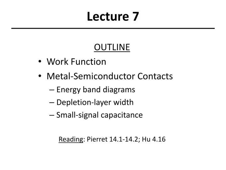
Lecture 7. OUTLINE Work Function Metal-Semiconductor Contacts Energy band diagrams Depletion-layer width Small-signal capacitance Reading : Pierret 14.1-14.2; Hu 4.16. Metal-Semiconductor Contacts. There are 2 kinds of metal-semiconductor contacts: rectifying “ Schottky diode ”

E N D
Lecture 7 OUTLINE • Work Function • Metal-Semiconductor Contacts • Energy band diagrams • Depletion-layer width • Small-signal capacitance Reading: Pierret 14.1-14.2; Hu 4.16
Metal-Semiconductor Contacts There are 2 kinds of metal-semiconductor contacts: • rectifying “Schottky diode” • non-rectifying “ohmic contact” EE130/230A Fall 2013 Lecture 7, Slide 2
Work Function E0: vacuum energy level R.F. Pierret, Semiconductor Fundamentals, Figure 14.1 FM: metal work function FS: semiconductor work function EE130/230A Fall 2013 Lecture 7, Slide 3
Ideal M-S Contact: FM <FS, n-type Band diagram instantly after contact formation: Equilibrium band diagram: EE130/230A Fall 2013 Lecture 7, Slide 4 R.F. Pierret, Semiconductor Fundamentals, Fig. 14.2
Ideal M-S Contact: FM >FS, n-type Band diagram instantly after contact formation: Equilibrium band diagram: qVbi = FBn– (Ec – EF)FB Schottky Barrier Height: n W EE130/230A Fall 2013 Lecture 7, Slide 5 R.F. Pierret, Semiconductor Fundamentals, Fig. 14.2
Effect of Interface States on FBn • Ideal M-S contact: FBn=FM– c • Real M-S contacts: A high density of allowed energy states in the band gap at the M-S interface “pins” EF to be within the range 0.4 eV to 0.9 eV below Ec FM FBn C. C. Hu, Modern Semiconductor Devices for ICs, Figure 4-35 EE130/230A Fall 2013 Lecture 7, Slide 6
Schottky Barrier Heights: Metal on Si • FBn tends to increase with increasing metal work function EE130/230A Fall 2013 Lecture 7, Slide 7
Schottky Barrier Heights: Silicide on Si Silicide-Si interfaces are more stable than metal-silicon interfaces and hence are much more prevalent in ICs. After metal is deposited on Si, a thermal annealing step is applied to form a silicide-Si contact. The term metal-silicon contact includes silicide-Si contacts. EE130/230A Fall 2013 Lecture 7, Slide 8
The Depletion Approximation The semiconductor is depleted of mobile carriers to a depth W • In the depleted region (0 x W ): r = q (ND – NA) Beyond the depleted region (x > W ): r = 0 EE130/230A Fall 2013 Lecture 7, Slide 9 R.F. Pierret, Semiconductor Fundamentals, Fig. 14.4
Electrostatics • Poisson’s equation: • The solution is: EE130/230A Fall 2013 Lecture 7, Slide 10 R.F. Pierret, Semiconductor Fundamentals, Fig. 14.4
Depletion Width, W At x = 0, V = -Vbi • W decreases with increasing ND EE130/230A Fall 2013 Lecture 7, Slide 11 R.F. Pierret, Semiconductor Fundamentals, Fig. 14.4
Voltage Drop across the M-S Contact • Under equilibrium conditions (VA = 0), the voltage drop across the semiconductor depletion region is the built-in voltage Vbi. • If VA 0, the voltage drop across the semiconductor depletion region is Vbi - VA. EE130/230A Fall 2013 Lecture 7, Slide 12 R.F. Pierret, Semiconductor Fundamentals, Fig. 14.3
Depletion Width, W, for VA 0 Last time, we found that At x = 0, V = - (Vbi- VA) • W increases with increasing –VA • W decreases with increasing ND EE130/230A Fall 2013 Lecture 7, Slide 13 R.F. Pierret, Semiconductor Fundamentals, Fig. 14.4
Charge Storage in a Schottky Diode • Charge is “stored” on both sides of the M-S contact. • The applied bias VA modulates this charge. R.F. Pierret, Semiconductor Fundamentals, Fig. 14.4 EE130/230A Fall 2013 Lecture 7, Slide 14
Small-Signal Capacitance • If an a.c. voltage va is applied in series with the d.c. bias VA, the charge stored in the Schottky contact will be modulated at the frequency of the a.c. voltage • displacement current will flow: EE130/230A Fall 2013 Lecture 7, Slide 15
Using C-V Data to Determine FB OnceVbi and ND are known, FBncan be determined: EE130/230A Fall 2013 Lecture 7, Slide 16
Ideal M-S Contact: FM >FS, p-type p-type semiconductor Band diagram instantly after contact formation: Equilibrium band diagram: EE130/230A Fall 2013 Lecture 7, Slide 17 R.F. Pierret, Semiconductor Fundamentals, p. 482
Ideal M-S Contact: FM <FS, p-type p-type semiconductor Band diagram instantly after contact formation: Equilibrium band diagram: Schottky Barrier Height: FBp qVbi = FBp– (EF – Ev)FB W EE130/230A Fall 2013 Lecture 7, Slide 18 R.F. Pierret, Semiconductor Fundamentals, p. 482
W for p-type Semiconductor p-type semiconductor At x = 0, V = Vbi+ VA • W increases with increasing VA • W decreases with increasing NA EE130/230A Fall 2013 Lecture 7, Slide 19
Summary Ec Ec EF EF Ev Ev Ec EF EF Ev Ev R.F. Pierret, Semiconductor Fundamentals, p. 481 For rectifying contacts: small-signal capacitance EE130/230A Fall 2013 Lecture 7, Slide 20
Summary: Rectifying Contacts • Schottky barrier height, FB: • Energy barrier that must be surmounted in order for a carrier in the metal to enter the semiconductor • Built-in potential, qVbi: FBn-(EC-EF)FB for n-type Si, FBp-(EF-Ev)FB for p-type Si • Ideally qVbi is equal to the work function difference between the metal and semiconductor. In practice, for Si: FBn (2/3)EG and FBp (1/3)EG EE130/230A Fall 2013 Lecture 7, Slide 21