Download
1 / 8
80 likes | 100 Views
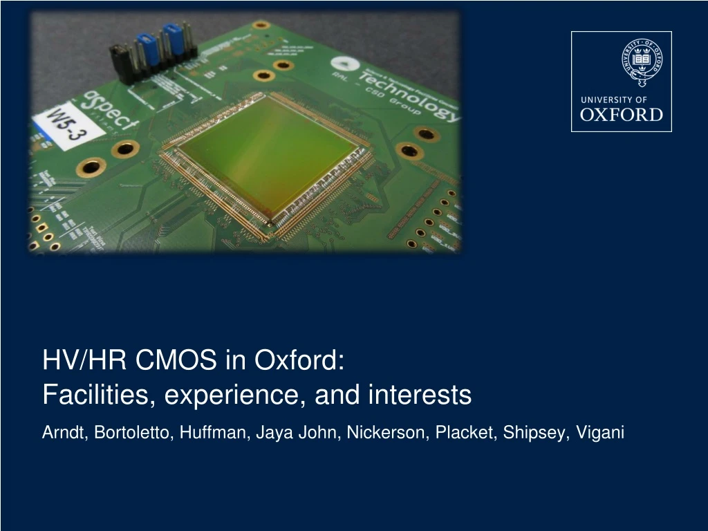
HV/HR CMOS in Oxford: Facilities, experience, and interests Arndt, Bortoletto, Huffman, Jaya John, Nickerson, Placket, Shipsey, Vigani. Oxford Particle Physics Microstructure Detector Laboratory - OPMD. Currently Under construction – expected completion in Oct 2015

E N D
HV/HR CMOS in Oxford: Facilities, experience, and interests Arndt, Bortoletto, Huffman, Jaya John, Nickerson, Placket, Shipsey, Vigani
Oxford Particle Physics Microstructure Detector Laboratory - OPMD Currently Under construction – expected completion in Oct 2015 Focused on generic R&D and ITK Strip/Pixel Module production Clean Rooms • 160 m2 of class 10,000 clean room • 35 m2 of class 100 clean room • Vacuum, Dry Compressed Air, Nitrogen & DI water as piped services Equipment • Semiprobe 300mm probe station with thermal chuck (delivery this month) • Hesse Bondjet 820 automatic wire bonder (delivery expected Oct/Nov) • Dage 4000Plus pull tester (Oct/Nov) • OGP CNC500 Smartscope optical metrology system (Oct/Nov) • Keyance VHX500 digital inspection microscope (Oct/Nov) • Weiss Thermal chamber WTL100 (+50oC –> -50oC) (Oct/Nov) • Henniker Bench top Plasma Cleaner (Oct/Nov) • Aerotech pick and place assembly gantry (Sept/Oct) • Nordson EFD Glue Robot (Delivered this week) HV-CMOS Infrastructure
Oxford Particle Physics Microstructure Detector Laboratory - OPMD Currently Under construction – expected completion in Oct 2015 Focused on generic R&D and ITK Strip/Pixel Module production Clean Rooms • 160 m2 of class 10,000 clean room • 35 m2 of class 100 clean room • Vacuum, Dry Compressed Air, Nitrogen & DI water as piped services Equipment • Semiprobe 300mm probe station with thermal chuck (delivery this month) • Hesse Bondjet 820 automatic wire bonder (delivery expected Oct/Nov) • Dage 4000Plus pull tester (Oct/Nov) • OGP CNC500 Smartscope optical metrology system (Oct/Nov) • Keyance VHX500 digital inspection microscope (Oct/Nov) • Weiss Thermal chamber WTL100 (+50oC –> -50oC) (Oct/Nov) • Henniker Bench top Plasma Cleaner (Oct/Nov) • Aerotech pick and place assembly gantry (Sept/Oct) • Nordson EFD Glue Robot (Delivered this week) HV-CMOS Infrastructure
CMOS replacement of sensors • Participating in the evaluation of HV-HR CMOS as a sensor replacement • Our activities up to now focused on the evaluation of strip • Amplifiers and comparators could be on sensor but the rest of digital processing, command I/O, trigger pipelines, etc will go into a readout ASIC • Transmit high-speed information instead of individual analog signals to readout ASICs. • The active area is pixelated, with connections to the periphery that can yield 2D coordinates • Looking at ~40 mm pitch and 800 mm length of pixel • Max reticle sizes are ~2x2 cm2. Therefore rows of 4-5 chips could be the basic units (yield performance is critical here). • R&D with two foundries AMS and TJ - Pixel efforts have more, e.g. L-foundry • Cost savings. • Faster construction • Less material in the tracker. HV-CMOS Infrastructure
HVStrip 1 – Ivan Peric (Karlsruhe/KIT) • AMS35 Technology • 22x2 pixels, 40x400 μm2 each, 750 μm total thickness Fe55 Calibration Test beam at DESY With 3, 4, and 5 GeV Electrons at different Single spectrum Two regions: linear transistor (left) and enclosed transistor (right) Telescope integration could lead to better understanding of the performance including charge sharing Gain map HV-CMOS Infrastructure
Hardware development • Developed electronics for testing HVStripV1 chip on behalf of Strip CMOS collaboration • Motherboard (green) for readout electronics and connectors • Daughterboard (yellow) for low-activation chip fanout, to favour irradiation • Currently developing hardware for testing HV and HR “CHESS” Strip CMOS detectors • HV-CHESS-1 daughterboard being manufactured this week • 79 output channels of varied active pixels and amplifiers HV-CMOS Infrastructure
Proton irradiation The set-up • Samples irradiated with 27 MeV protons at Birmingham • Irradiation divided in 4 steps of 15 minutes • Total irradiation of 8.8x10¹⁴ and 7.6x10¹⁴ neq/cm2 respectively • After annealing (60° for 80 minutes) Sr90 spectrum could be observed (measurements done at Cambridge) Source Chip Scope Scintillator Landau-Gauss plus with exponential Bias 60 V • Exponential function to parameterize the observed background • MIP peak observed, lower MPV than unirradiated (~60%) HV-CMOS Infrastructure
Interests and Possible Contributions • We are especially interested in: • Task 6.3 Sensor development: • Characterise test-structures and sensors using electrical measurements, lasers, sources and test beams • Perform irradiation campaigns to validate the radiation hardness of each process technology and sensor design • Task 6.4 Hybridisation • Perform basic R&D on capacitive interconnection • Setup production facilities for full-prototype assemblies (chips on test boards) • Deliver full assemblies to all participating projects • Investigate options for future industrialisation of the interconnection process HV-CMOS Infrastructure