Download
1 / 20
200 likes | 288 Views
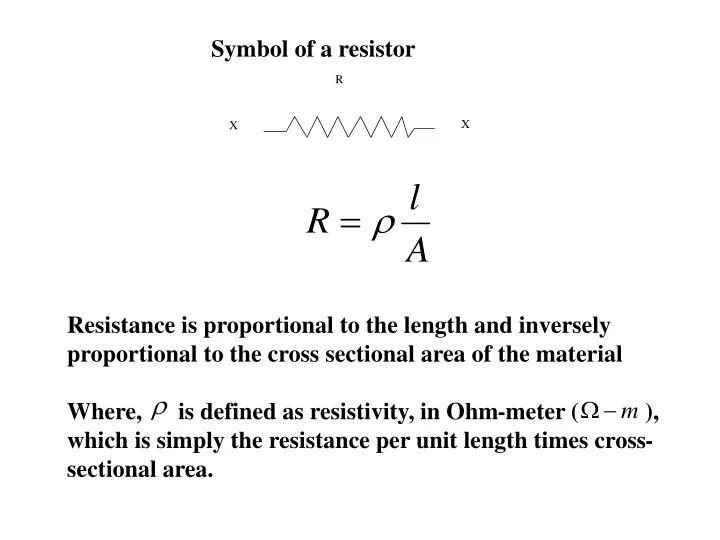
R. X. X. Symbol of a resistor. Resistance is proportional to the length and inversely proportional to the cross sectional area of the material Where, is defined as resistivity, in Ohm-meter ( ), which is simply the resistance per unit length times cross-sectional area. X. X.

E N D
R X X Symbol of a resistor Resistance is proportional to the length and inversely proportional to the cross sectional area of the material Where, is defined as resistivity, in Ohm-meter ( ), which is simply the resistance per unit length times cross-sectional area.
X X Y Y (a) (b) Series connection Parallel connection Resistances connected in series and parallel are calculated using the following formula.
L X Y Symbol Purpose-made conductor coils are called inductors. When current flows electromagnetic field is established. The electromagnetic lines of force surrounds the conductor and the magnetic lines of force becomes concentrated. When the current changes, the electromagnetic field changes accordingly and the changing electromagnetic field causes an induced voltage in a direction in opposite to the flow of current. This property is referred to as inductance.
Electrode-1 X C Surface-1 Dielectric material Surface-2 Y Electrode-2 A capacitor is an energy storage passive component. The term capacity signifies "what is the capacity of the surfaces in holding the electrical charges." It stores charge and hence electric field energy. The equivalent capacitance of a series combination is always less than any individual capacitance in the combination and can be expressed using the following equation. On the other hand, the parallel connection adds up all the individual capacitances
Inductive reactance Inductive reactance Frequency Inductance (a) Capacitive reactance Capacitive reactance Frequency Capacitance (b) Inductive reactance versus inductance and frequency curve. Capacitive reactance versus capacitance and frequency curve.
A piece of intrinsic Semiconductor material Terminal Terminal B A _ Flow of current (a) (b) (c) Flow of electrons p-type Semiconductor material Terminal Terminal B A _ Flow of current Immobile Acceptor atoms (Trivalent) Flow of holes n-type Semiconductor material _ _ Terminal _ _ _ Terminal _ _ _ B A _ _ _ _ _ _ _ _ _ Flow of current Immobile Donor atoms (Pentavalent) Flow of electrons If the donors are added, the intrinsic semicond-uctor becomes n-type semiconductor and if the acceptors are added it becomes p-type semicon-ductor. n-type semico-nductor materials have loosely-attached free-electrons and p-type semiconductor materials have loosely-attached free-holes. The electrons and holes, in the respective extrinsic semi conductors, are called charge carriers
Depletion layer Majority carriers (holes) Majority carriers (electrons) p-type n-type Electrode Electrode Uncovered immobile atoms Uncovered immobile atoms Potential barrier (a) + + + - - - n-type p-type (b) Semiconductor diodes or junction diodes are two terminal electronic devices made up of two types of semiconductor materials. One side of the device has n-type material and the other side has p-type. A depletion layer is a layer in which the charge carriers are absent
Reverse-biased p-n junction diode Forward-biased p-n junction diode - + + - Voltage source Voltage source Current is mA Current is mA (a) (b) Voltage in volts Voltage in volts I is the diode current, q is charge of the carriers, k is a constant, V is the applied voltage T is temp. in degrees K The behavior of a junction diode is such that it offers a low resistance to electric current in one direction and a high resistance to it in the reverse direction. This property is a requirement in the context of signal manipulation and processing. The current equation in the diode is given above.
Capacitance Current Negative coefficient of resistance Reverse voltage Diode voltage Varacter Tunnel Varactor exploits the depletion layer in terms of a parallel plate capacitor, whose capacitance is controlled by applying reverse voltage. The capacitance across the junction is inversely proportional to the width of the depletion layer. The varactors useful for designing VCO, FM modulators and demodulators and tuning circuits. In the tunnel diode, the current through the device decreases as the voltage increases within a certain range This property, known as negative resistance, makes it useful as a switch and oscillators.
+ + - - Amplitude Amplitude Time Time (c) Diode (b) input Output Amplitude Amplitude Common terminal called GROUND (Common to both input and Output) Time Time (a) (d) (a) In general, junction diodes are referred to as rectifiers because when an alternating signal (voltage or current) say a sinusoidal or rectangular signal is applied (assuming ideal diode) the output would be a signal containing only positive half-cycles.
C C B B p-n-p (Symbol) n-p-n (Symbol) C E E B (c) (d) Output input E Common-emitter configuration Emitter (E) Collector (C) Emitter (E) Collector (C) P N P N P N • A pnp transistor • (b) An npn transistor • (c) Symbol of a pnp • (d) Symbol of npn Base (B) Base (B) (a) (b) E C n-p-n C input B Input Output n-p-n n-p-n Output B E Common-collector configuration Common-base configuration (e) (g) (f) (e) The common emitter configuration of an n-p-n transistor (f) the common collector configuration of an n-p-n transistor (g) The common base configuration of an n-p-n transistors
In mA In mA in mA in mA SATURATION REGION in mA ACTIVE REGION Cut- Off Region In volts In volts (b) (a) The output characteristics of a typical transistor is shown. The shadow portion of the figure provides much information about the transistor. The entire quadrant is divided into three regions, the active region, the saturation region, and the cut-off region. Each point in the quadrant is called an operating point or Q-point of the transistor.
E B C Emitter current Collector current Base current The collector current is the sum of the emitter current and the base current.
- Biasing voltage (source) - Resistance at input circuit - Collector to Emitter voltage - Biasing resistances - Load resistance - Base to Emitter voltage - Blocking capacitor (it block dc component) - Feedback resistance -Feedback capacitor - Coupling capacitor (to next stage) +Vcc The characteristic of a transistor is such that a small voltage change in the base-emitter junction will produce large current change in the collector and emitter, whereas small changes in the collector-emitter voltage have little effect on the base. A typical transistorized amplifying circuit is given. C B n-p-n E + _ Output + _ input Common-emitter configuration Ground
Drain (D) _ + n-channel Depletion layer Depletion layer (Gate (G) P-type P-type _ + n-type Source (S) Junction Field Effect Transistor (JFET) or simply FET are of two types, p-channel FET and n-channel FET. In each case, a semiconductor bar called channel of one type of semiconductor material is located inside a bulk of material of the other kind. Bipolar junction transistors have low input impedance small high-frequency gain, and are to some extend non-linear. However, high input impedance is desirable for low power consumption. FET overcomes this problem.
Equivalent diode Cathode Anode Emitter current Base-2 E E + - Emitter + - A p A + - n Base-1 Characteristics UJT Symbol Equivalent circuit (c) (d) (a) Ground (b) A typical construction of a transistor defines itself as a unijunction transistor (UJT), a transistor with only one junction and three terminals. UJT exhibits a negative resistance characteristic as can be seen from the V-I plot This switching feature can be exploited in designing oscillators.
SCR current Anode Anode Forward conduction p n p n J1 Forward breakover voltage Reverse breakdown voltage + - + - J2 Gate Gate voltage J3 Gate Cathode Cathode (c) Characteristics Ground SCR Symbol (a) (b) SCR stands for Silicon Controlled Rectifier. SCRs are four-layered diodes and shows negative resistance characteristics. It has three junctions and three terminals. The application of a forward voltage is not enough for conduction since the junction is reverse biased. A gate signal can control the conduction of the rectifier.
Positive supply Inverting terminal _ Output + Noninverting terminal Negative supply Input signal can either be connecter to inverting or noninverting terminal Operational Amplifiers (OPAMP) are analog ICs and are basically amplifiers, but can be configured in a variety of ways in order to design low- and high-pass filters, differential amplifiers, oscillators, impedance matching circuits (unit follower), sample and hold (S/H) circuits, current limiters, rectifiers, instrumentation amplifiers, comparators, zero crossing detectors, and so on.
- + - + + - + - + - + - Open-loop (Closed-loop) (a) (b) The gain of the OPAMP is defined as the ratio of output voltage to the input voltage. Two different types of gains are encountered in the OPAMP: open-loop gain and closed loop gain. Open-loop gains again are of two types, open-loop differential mode gain and open-loop common mode gain