Download
1 / 24
420 likes | 1.22k Views
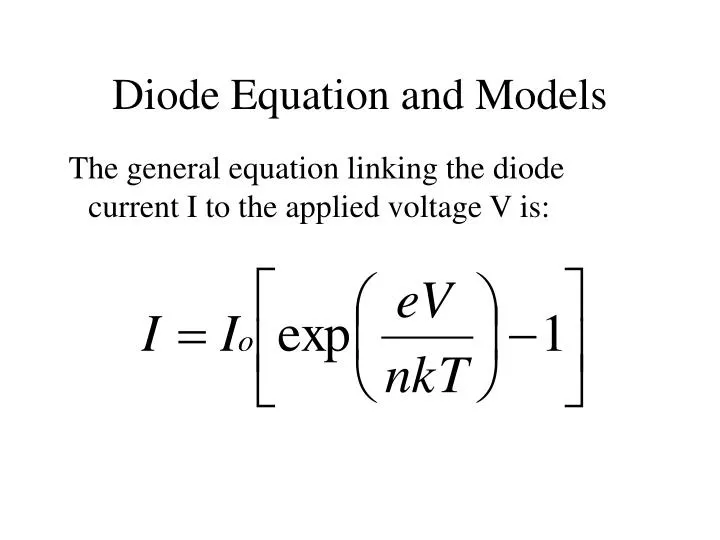
Diode Equation and Models. The general equation linking the diode current I to the applied voltage V is: . Diode Equation and Models. Here: I o is the reverse saturation current. k is Boltzmann's constant= 1.38 x 10 -23 JK -1. T is the working temperature in Kelvin.

E N D
Diode Equation and Models The general equation linking the diode current I to the applied voltage V is:
Diode Equation and Models • Here: • Io is the reverse saturation current. • k is Boltzmann's constant= 1.38 x 10⁻²³ JK-1. • T is the working temperature in Kelvin. • e is the magnitude of the electronic charge. • n is called the ideality factor. (n= 1 from theory. From experiments on silicon diodes n= 2 at low current and 1 for large currents).
Diode Equation and Models • As an exercise satisfy yourself that this explains the facts discussed in the Semiconductor Diodes section of the module. (The ‘exponential’ term corresponds to majority carrier flow whilst the ‘–1’ term relates to the ‘reverse saturation’ component) • You can now tackle questions 1-4 on Example Sheet1!
Diode Equation and Models • By plotting out this equation on a ‘practical scale’ we see that to a good approximation
Diode Equation and Models • Diode eqn
Diode Equation and Models • An ideal diode would show an abrupt transition from perfectly conducting (diode short circuit) to perfectly non-conducting (diode open circuit) states at 0V I V
I OFF ON Smith/Dorf symbol for ideal diode V Diode Equation and Models • It acts as switch since • In the ON state it is a short and in the OFF state it is open circuit
I V 0.6 Diode Equation and Models • An silicon diode approximates this ideal but the transition from conducting to non-conducting circuit states is at around 0.6V because of the barrier potential. This voltage is called the cut-in voltage
Diode Equation and Models • Experiment
I V 0.6 Diode Equation and Models • A closer approximation to the diode I-V equation (experiment) also includes the bulk resistance. This gives the diode’s I-V curve a finite slope above cut-in.
Diode Equation and Models • Diodes formed in other materials have different cut-in voltages. • Diodes breakdown for large reverse bias (Breakdown voltage)
Diode Equation and Models • We are now in a position to draw some models that represent diode behaviour. • We can use these models instead of the diode equation in circuit analysis • Later on in the Module we will be developing similar models (or equivalent circuits) to represent the behaviour of transistors when they are used as linear amplifiers.
Diode Equation and Models • Diode circuit symbol Anode Cathode p n
Diode Equation and Models • BS3939, IEC symbol (For information only, Smith and Dorf’s symbols will be used in the module)
Diode Equation and Models • In forward bias the equivalent circuit is a forward bias drop (Vc ~ 0.6V) in series with a small (forward) resistance. I + - V V 0.6 R f VC
I V 0.6 Diode Equation and Models • In many cases Rf can be ignored. 0.6V
Diode Equation and Models • In reverse bias (strictly in the ‘off’ state below Vc) the diode can be represented by a very large resistor Rr. • We shall assume Rr. to be infinitely large so that the piecewise linear model for the diode is:
Diode Equation and Models • Incremental Diode Model • Another important principle that we will need for transistor analysis is that of the‘incremental modelling’ of a non-linear device. • Basically this assumes the diode I-V curve is linear for small variations in I and V about some operating or bias point. (Also known as the ‘Q’ or quiescent point.)
Diode Equation and Models • We introduce important notation used throughout the module. As noted, the (small) a.c. signal sits on top of a d.c. bias level. • Lower-case symbols are used for the time varying signals (i, v). • Upper-case symbols are used for the d.c. bias levels (I, V).
I, i I, i i Q t V, v VQ V, v v t Diode Equation and Models
Diode Equation and Models • The diode is biased to operate about a point Q on the I-V curve • The small a.c. signal is superimposed on this bias. • The diode can then be modelled by a resistance equal to the inverse slope of the tangent to the bias point (Linear approximation to diode curve)
We will, in the examples class, use the diode equation to show that, for an ideality factor of 1, the dynamic (small signal) resistance is: Diode Equation and Models
Zener Diode • This is simply a diode whose breakdown voltage is controlled to be a specific value. • It finds wide use in limiting and voltage regulator circuits (see diode application section of the module)