Download
1 / 14
140 likes | 145 Views
This article explores analog and digital signals, binary number system, and Boolean algebra in relation to solids and semiconductor devices. It covers topics such as logic gates, truth tables, and electrical circuits for logic operations.

E N D
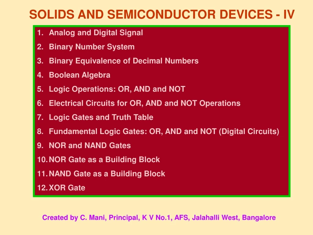
SOLIDS AND SEMICONDUCTOR DEVICES - IV • Analog and Digital Signal • Binary Number System • Binary Equivalence of Decimal Numbers • Boolean Algebra • Logic Operations: OR, AND and NOT • Electrical Circuits for OR, AND and NOT Operations • Logic Gates and Truth Table • Fundamental Logic Gates: OR, AND and NOT (Digital Circuits) • NOR and NAND Gates • NOR Gate as a Building Block • NAND Gate as a Building Block • XOR Gate Created by C. Mani, Principal, K V No.1, AFS, Jalahalli West, Bangalore
V V 0 t t 0 Analogue signal Digital signal A continuous signal value which at any instant lies within the range of a maximum and a minimum value. A discontinuous signal value which appears in steps in pre-determined levels rather than having the continuous change. V = V0 sin t (5 V) 1 0 1 0 1 0 1 0 1 (5 V) (0 V) (-5 V) Digital Circuit: An electrical or electronic circuit which operates only in two states (binary mode) namely ON and OFF is called a Digital Circuit. In digital system, high value of voltage such as +10 V or +5 V is represented by ON state or 1 (state) whereas low value of voltage such as 0 V or -5V or -10 V is represented by OFF state or 0 (state).
Binary Number System: A number system which has only two digits i.e. 0 and 1 is known as binary number system or binary system. The states ON and OFF are represented by the digits 1 and 0 respectively in the binary number system. Binary Equivalence of Decimal Numbers: Decimal number system has base (or radix) 10 because of 10 digits viz. 0, 1, 2, 3, 4, 5, 6, 7, 8 and 9 used in the system. Binary number system has base (or radix) 2 because of 2 digits viz. 0 and 2 used in the system.
● ● ● ● E Boolean Algebra: George Boole developed an algebra called Boolean Algebra to solve logical problems. In this, 3 logical operations viz. OR, AND and NOT are performed on the variables. The two values or states represent either ‘TRUE’ or ‘FALSE’; ‘ON’ or ‘OFF’; ‘HIGH’ or ‘LOW’; ‘CLOSED’ or ‘OPEN’; 1 or 0 respectively. OR Operation: OR operation is represented by ‘+’.Its boolean expression is Y = A + BIt is read as “Y equals A OR B”.It means that “if A is true OR B is true, then Y will be true”. A Truth Table Y B
● ● ● ● ● ● ● E E AND Operation: AND operation is represented by ‘.’ Its boolean expression is Y = A . B It is read as “Y equals A AND B”. It means that “if both A and B are true, then Y will be true”. Truth Table A B Y NOT Operation: NOT operation is represented by ′ or ¯.Its boolean expression is Y = A′ or ĀIt is read as “Y equals NOT A”.It means that “if A is true, then Y will be false”. Truth Table A Y
Logic Gates: The digital circuit that can be analysed with the help of Boolean Algebra is called logic gate or logic circuit. A logic gate can have two or more inputs but only one output. There are 3 fundamental logic gates namely OR gate, AND gate and NOT gate. Truth Table: The operation of a logic gate or circuit can be represented in a table which contains all possible inputs and their corresponding outputs is called a truth table. If there are n inputs in any logic gate, then there will be n2possible input combinations. 0 and 1 inputs are taken in the order of ascending binary numbers for easy understanding and analysis. Eg. for 4 input gate
● ● + ● ● 5 V ● ● RL ● + 5 V E E E E A Y B ● ● ● Digital OR Gate: The positive voltage (+5 V) corresponds to high input i.e. 1 (state).The negative terminal of the battery is grounded and corresponds to low input i.e. 0 (state). A D1 B Y D2 Case 1:Both A and B are given 0 input and the diodes do not conduct current. Hence no output is across RL. i.e. Y = 0 Case 2: A is given 0 and B is given 1. Diode D1 does not conduct current (cut-off) but D2 conducts. Hence output (5 V)is available across RL. i.e. Y = 1 Truth Table Case 3:A is given 1 and B is given 0. Diode D1 conducts current but D2 does not conduct. Hence output (5 V)is available across RL. i.e. Y = 1 Case 4:A and B are given 1. Both the diodes conduct current. However output (only 5 V)is available across RL. i.e. Y = 1
● ● D1 + ● ● 5 V ● ● RL D2 ● + 5 V + 5 V E E E E ● ● ● A Y B Digital AND Gate: A Case 1:Both A and B are given 0 input and the diodes conduct current (Forward biased). Since the current is drained to the earth, hence, no output across RL. i.e. Y = 0 B Y Case 2: A is given 0 and B is given 1. Diode D1 being forward biased conducts current but D2 does not conduct. However, the current from the output battery is drained through D1. So, Y = 0 Case 3:A is given 1 and B is given 0. Diode D1 does not conduct current but D2 being forward biasedconducts . However, the current from the output battery is drained through D2.Hence, no output is available across RL. i.e. Y = 0 Truth Table Case 4:A and B are given 1. Both the diodes do not conduct current. The current from the output battery is available across RL and output circuit. Hence, there is voltage drop (5 V) across RL. i.e. Y = 1
C N P N B RL E ● ● ● Rb Y ● ● + + 5 V 5 V ● ● E E E E ● Y ● ● A Digital NOT Gate: NPN transistor is connected to biasing batteries through Base resistor (Rb) and Collector resistor (RL). Emitter is directly earthed. Input is given through the base and the output is tapped across the collector. Case 1:A is given 0 input. In the absence of forward bias to the P-type base and N-type emitter, the transistor is in cut-off mode (does not conduct current). Hence, the current from the collector battery is available across the output unit. Therefore, voltage drop of 5 V is available across Y. i.e. Y= 1 A Truth Table Case 2:A is given 1 input by connecting the +ve terminal of the input battery. P-type base being forward biased makes the transistor in conduction mode. The current supplied by the collector battery is drained through the transistor to the earth. Therefore, no output is available across Y. i.e. Y = 0
Y = (A + B)′ A ● C ● ● B N P N B RL E A ● ● ● ● ● D1 Rb Y + ● ● ● 5 V B ● ● + RL 5 V D2 ● ● + E E 5 V E E ● E E ● A ● ● Y = (A + B)′ ● A + B B NOR Gate: Symbol: Circuit: Truth Table
Y = (A . B)′ A C B A ● ● D1 N P + ● ● N B RL 5 V E B ● ● RL D2 ● ● ● + Rb Y 5 V E E + + 5 V 5 V ● ● E E E E ● ● ● ● ● ● ● ● ● A A . B Y = (A . B)′ B NAND Gate: Symbol: Circuit: Truth Table
A ● ● ● B (A + B)′ ● Y = A + B A′ A ● A′ ● ● ● Y = A . B B′ B ● B′ ● ● ● ● A ● Y = A′ NOR Gate as a Building Block: OR Gate: AND Gate: NOT Gate:
A B A′ A B A′ ● B′ Y = A + B B′ Y = A . B ● ● ● ● ● ● ● ● ● ● ● ● ● A Y = A′ NAND Gate as a Building Block: OR Gate: AND Gate: (A . B)′ NOT Gate:
A′ A′B A Y = A′B + AB′ = A B B A AB′ B B′ ● ● ● ● ● ● ● ● ● ● A B Y = A B XOR Gate: End of S & SCD - IV