Download
1 / 26
260 likes | 276 Views
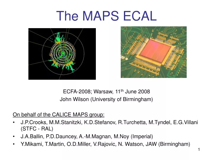
The MAPS ECAL. ECFA-2008; Warsaw, 11 th June 2008 John Wilson (University of Birmingham) On behalf of the CALICE MAPS group: J.P.Crooks, M.M.Stanitzki, K.D.Stefanov, R.Turchetta, M.Tyndel, E.G.Villani (STFC - RAL) J.A.Ballin, P.D.Dauncey, A.-M.Magnan, M.Noy (Imperial)

E N D
The MAPS ECAL ECFA-2008; Warsaw, 11th June 2008 John Wilson (University of Birmingham) On behalf of the CALICE MAPS group: • J.P.Crooks, M.M.Stanitzki, K.D.Stefanov, R.Turchetta, M.Tyndel, E.G.Villani (STFC - RAL) • J.A.Ballin, P.D.Dauncey, A.-M.Magnan, M.Noy (Imperial) • Y.Mikami, T.Martin, O.D.Miller, V.Rajovic, N. Watson, JAW (Birmingham)
Effect of pixel size Weighted no. pixels/event >1 particle/ pixel Incoming photon energy (GeV) Using pixels in calorimeters? • Determine energy by counting tracks in a shower rather than measuring the pulse heights produced in the samples. • Swap ~0.5x0.5 cm2 Si pads for pixels • at most one particle per pixel if linearity is to • be preserved • binary readout: 1 if input pulse exceeds a • comparator threshold. • At 500 GeV, shower core density is ~100/mm2 (1 particle per 100 x 100 m2 ) • pixel size = 50 x 50 m2 ensures a low probability of >1 hit in pixel. 50m General advantages with MAPS (Monolithic Active Pixel Sensors): readout electronics is an integral part of sensor high density – excellent for sampling calorimeters? 100m JAW; ECFA 2008, WARSAW
Use 0.18m CMOS technology; Readout electronics on surface of pixel; 12 micron epitaxial layer (ionisation deposited here is collected); 300 micron substrate (mechanical support only; ionisation here is not collected); Electrons collected by N wells (diodes AND N wells beneath PMOS electronics). Avoid absorption in N wells by surrounding them with a deep P well (which reflects electrons back into the epitaxial layer) INMAPS process Charge collected by diffusion (not drift) Depletion layers near diodes are tiny (1.8V applied few microns) MAPS charge collection
Simulating the deep P well • Central N well absorbs half charge leading to difficult operation; serious degradation • Deep P well gives reasonable range of threshold. • Clear advantage in implementing deep P well • BUT novel process JAW; ECFA 2008, WARSAW
pink = nwell (absorbing charge) grey = deep p-well added to block the charge absorption (INMAPS process) Deep P well implementation Shaper • All pixels contain 4 collection diodes, each 1.8micron diameter and located 8.5 microns from corner along a diagonal • preShape RC shaping; recovers before next hit) • preSample (self reset before next hit) Each with: • two variants of Capas and same comparator logic • Mask bit • 4 Trim bits Sampler JAW; ECFA 2008, WARSAW
Shaper Sampler ASIC 1.0 Capa 1 • 168 x 168 pixels • 10mm x 10mm • 79.4 mm2 sensitive area • of which 11.1% is dead (logic etc) • ordered April 2007; delivered July 2007. • As a binary device, we can investigate noise, pedestal etc by carrying out threshold scans: i.e. varying the global comparator threshold and counting the number of hits per pixel. Capa 2
Threshold scans of individual pixels • Means significantly different but RMS is similar • RMS of theshold peak Noise • 5 Threshold Units 40 electrons – as expected JAW; ECFA 2008, WARSAW
Crosstalk between pixels Scan one pixel at a time; all others off. Scan one pixel at a time; all others on. • Effect of all pixels (other than the one being scanned) is to increase the general noise around zero. JAW; ECFA 2008, WARSAW
Trimming the thresholds After Before • Trimming reduces the range of pixel thresholds but not enough. (The spread in thresholds is still much larger than the width of a typical threshold scan). • More dynamic range is required (i.e. 6 trim bits) in order to bring all thresholds into close proximity. • Difficult to find a global threshold to allow reliable efficiency measurements complicatedtest beam analysis
Beam tests at DESY • < one week in mid-December 2007; very tight schedule; last opportunity before long shutdown. • Electron beam: 2-6 GeV • 4 sensors plus up to 10 absorber sheets (W; 3mm) all aligned precisely • Signals from small scintillators upstream and downstream recorded also. JAW; ECFA 2008, WARSAW
Test beam at DESY JAW; ECFA 2008, WARSAW
Test beam results: tracks seen • Observe strong correlations in x and y in adjacent planes • Tracks picked out by event display • Due to large natural spread in thresholds, it was not feasible to trim the pixels to a uniform response • as the global threshold was set too high (to keep the hit rate reasonable), the estimated efficiency is very low • With all pixels set with the appropriate trims, the efficiency is expected to be high JAW; ECFA 2008, WARSAW
Other tests (ongoing) • Radioactive sources : Fe-55 (5 keV X-rays) and Sr-90 (>2MeV electrons) uniformity (e.g. of efficiency vs threshold) over the whole sensor; uniformity of threshold and gain. • Cosmic rays absolute mip calibration. • Lasers uniformity of gain from pixel to pixel; charge diffusion and crosstalk; comparison with simulation. JAW; ECFA 2008, WARSAW
50 m 1 21 Cell size: 50 x 50 m2 Whole 3*3 array with neighbouring cells is simulated, and the initial MIP deposit is inputted on 21 points (sufficient to cover the whole pixel by symmetry) Simulation of charge diffusion Diodes Central N well Example of pessimistic scenario of a central N-well eating half of the charge JAW; ECFA 2008, WARSAW
Charge sharing between pixels • Infra red laser (spot size: few microns) illuminates grid of 21 points (5 micron spacing) in the central pixel of a set of 3 x 3 pixels. [Same grid as used by simulation, discussed earlier]. • For each position of the laser, take threshold scans of the 3x3 pixels. JAW; ECFA 2008, WARSAW
Charge diffusion: summing 3x3 pixels Diode • Excellent agreement between data and simulation both with and • without the deep P well. • With no deep P well, the diodes see signal predominantly from locations nearest to them (i.e. 9,13,14,18, 19, 20 – all near a group of diodes and furthest from the N well.
Charge sharing: deep P well Simulation Data • Reasonable qualitative agreement; e.g. cell 4 has peaks at 3,6,10,15 (all locations closest to the cell) • Cells 2, 3, 5 and 6 all have the same response at location 20 since this point is on the corner of the 4 cells,
Charge sharing: no deep P well data simulation • Much greater variation with position of laser spot as ionisation is lost unless near a diode. JAW; ECFA 2008, WARSAW
Conclusions • Reasonable agreement between data and simulation gives confidence in predicted performance • Sensors are being tested at three labs gaining experience with binary system INMAPS sensors look encouraging way forward has become clear JAW; ECFA 2008, WARSAW
Next steps • Design ASIC 1.1 : 1. dispense with presamplers; preshapers only but still with the two capacitance variants 2. Implement a 6 bit trim (though space is tight on pixel) 3. Adjust the power distribution to reduce crosstalk, 4. Fix three minor faults in original version • Submit to foundry by mid-July; expect to receive chips by August/September 2008. JAW; ECFA 2008, WARSAW
Backup slides JAW; ECFA 2008, WARSAW
Tracking calorimeter 5050 μm2 MAPS pixels ZOOM SiD 16mm2 area cells JAW; ECFA 2008, WARSAW
50 m 1 21 Cell size: 50 x 50 m2 Whole 3*3 array with neighbouring cells is simulated, and the initial MIP deposit is inputted on 21 points (sufficient to cover the whole pixel by symmetry) Simulation of charge diffusion Diodes Central N well Example of pessimistic scenario of a central N-well eating half of the charge JAW; ECFA 2008, WARSAW
Sensors in test beam • Beam traverses triggering scints, then 2 + 2 preshapers and presamplers • mixture of shapers and samplers trimming to a consistent threshold very difficult JAW; ECFA 2008, WARSAW
Thresholds for groups of pixels • We see considerable variation in position of the threshold; also a marked difference between shapers and samplers. • Since a global threshold is applied to all pixels and each has its own distinct threshold, a 4 bit trim is provided for each pixel to bring its threshold into line. Shapers Samplers Shapers