Download
1 / 52
800 likes | 1.57k Views
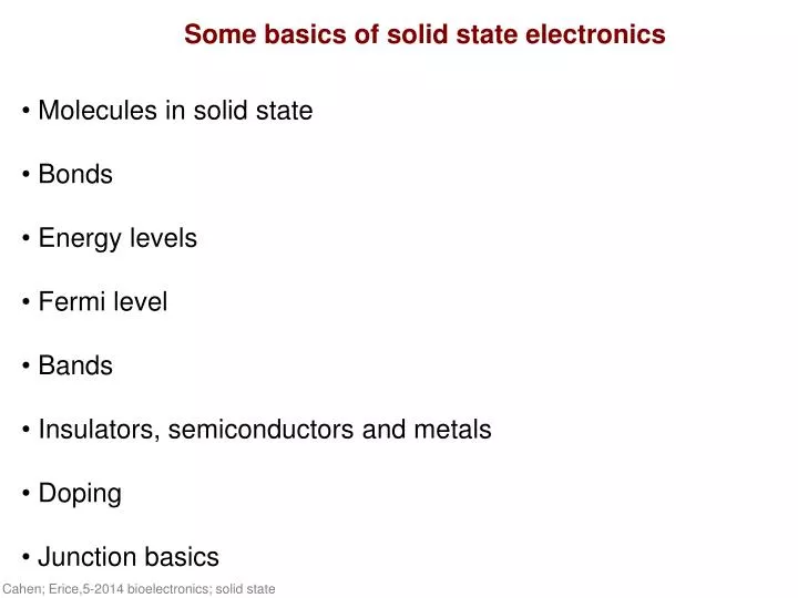
Some basics of solid state electronics. Molecules in solid state Bonds Energy levels Fermi level Bands Insulators, semiconductors and metals Doping Junction basics. The hydrogen molecule. H + H H 2. The hydrogen molecule.

E N D
Some basics of solid state electronics • Molecules in solid state • Bonds • Energy levels • Fermi level • Bands • Insulators, semiconductors and metals • Doping • Junction basics
The hydrogen molecule H + H H2
The hydrogen molecule r0 : distance between atoms where system’s energy is minimized H + H H2
Types of Bonding Ionic van der Waals Metallic Covalent Hydrogen High Melting Point Hard and Brittle Non conducting solid NaCl, CsCl, ZnS • Usually • 400-4000 kJ/mol LowMelting Point SoftandBrittle Usually Non-Conducting İce, organicsolids • Usually • 5-30 kJ/mol Low MeltingPoint Soft and Brittle Non-Conducting Ne, Ar, Kr and Xe • Usually • 2-4 kJ/mol Variable Melting Point Variable Hardness Conducting Fe, Cu, Ag • Usually • 75-1000 kJ/mol Very High Melting Point Very Hard Usually not Conducting Diamond, Graphite • Usually • 150-1100 kJ/mol
Vacuum Level E = 0 Empty States LUMO Fermi Level Energy Filled States HOMO A Small Molecule A Large Molecule Bulk Material An Atom Energy Levels Chemistry is controlled by the states around the filled/empty transition, i.e., the electronic charge neutrality level, around the …… Fermi Level Dan Thomas, Univ. Guelph, Canada http://www.chembio.uoguelph.ca/educmat/chem7234/
Large ΔE between filled and empty states Small, but non-zero ΔEbetween filled and empty states Infinitesimal energy difference (ΔE) between filled and empty states Valence Band Band Gap Core Bands Semiconductor Insulator Metal Bands distinguish different Electronic Materials Dan Thomas, Univ. Guelph, Canada http://www.chembio.uoguelph.ca/educmat/chem7234/
( c ) ( d ) ( b ) ( a ) y A C O N D U C T I O N B A N D y h y b y A p 3 E E n e r g y g a p , g s 3 y B S i A T O M V A L E N C E B A N D y B S i C R Y S T A L Inorganic semiconductors: energy bands Semiconductor crystal made of atoms that share electrons to form (at least partially) covalent bonds. The structure depends on the valencyof constituent atoms Ec: conduction band minimum Ev: valence band maximum y h y b Principles of Electronic Materials and Devices, S.O. Kasap, McGraw Hill. A. Kahn, Princeton
N N N N Z n N N N N Organic semiconductors: molecular levels Semiconductor crystal made of molecules held together by weak van der Waals forces. The electronic structure of the solid derives in large part from the molecular moiety. ZnPc Small molecules Pentacene Energy gap; 1-5 – 3.5 eV LUMO: lowest unoccupied molecular orbital HOMO: highest occupied molecular orbital A. Kahn, Princeton
Bands distinguish different Electronic Materials Conduction band Conduction band Valence band Semiconductor if Eg < 4-5 eV (@ RT) Remember: kBT @RT ≅ 26 meV ~ 200 cm-1
Fermi Level I • Each allowed energy level can be occupied by no more than • 2 e-s of opposite “spin”. • This means that, @ low temperatures, all available electronic energy levels in the material, up to a certain energy level will be occupied by 2 e-s . This is the Fermi level, EF. • The probability of e-s occupying a level @ energy E, @ a certain temperature, T, is given by the Fermi-Dirac distribution function, f(E):
Minimum energy to remove electron from Sample = Work Function E=0 (vacuum level) EF (Fermi level) Metal 1 Metal 2 Fermi Level II • focus on the electrons near the filled/empty boundary. • each material’s energy state distribution is unique; different EF. EF (Fermi level) the closer an electron is to the vacuum level, the weaker it is bound to the solid or, the more energetic is the electron Dan Thomas, Univ. Guelph, Canada http://www.chembio.uoguelph.ca/educmat/chem7234/
Potential energy and charge carrier distribution Semiconductor @ 0 K. No thermal excitation across the energy gap. Valence band: full; conduction band: empty; Systems always want to minimize energy; electrons go to lowest potential energy configuration (valence band) Filled bands do not conduct; @ 0 K semiconductor is insulator Electron potential energy Conduction band CBM EG EF VBM Valence band position Intrinsic (undoped) semiconductor @ finite T: Some thermal excitation of electrons across EG Electrons in conduction, holes in valence band (ni = intrinsic carrier concentration; Nc, Nv= effective density of states @ conduction, valence band edges) Partially filled bands conduct finite conductivity Electron potential energy Conduction band CBM EF EG Valence band VBM Valence band position A. Kahn, Princeton
– + – + – + – + – + electron flow leads to charge separation Contact potential difference Fermi level equal throughout sample @ electronic equilibrium Two Conductors in Contact Dan Thomas, Univ. Guelph, Canada http://www.chembio.uoguelph.ca/educmat/chem7234/
Metal in an Electrolyte Solution For electronic equilibrium in the system, charge is transferred to equilibrate (solid’s) Fermi level with the (solution) redox potential, producing charge separation and a contact potential difference. Redox potential = Electrochemical potential of the electron = Fermi level + – + – + – Fermi levels are aligned Dan Thomas, Univ. Guelph, Canada http://www.chembio.uoguelph.ca/educmat/chem7234/
An Ion in Solution ion’s electronic structure: HOMO, LUMO, HOMO-LUMO gap. Lowest Unoccupied Molecular Orbital HOMO-LUMO Gap “Fermi” level Highest Occupied Molecular Orbital Dan Thomas, Univ. Guelph, Canada http://www.chembio.uoguelph.ca/educmat/chem7234/
Electrochemical Thermodynamics Every substance has a unique propensity to contribute to a system’s energy. We call this property Chemical Potential. m When the substance is a charged particle (such as an electron or an ion) we must include the response of the particle to an electrical field in addition to its Chemical Potential. We call this Electrochemical Potential. These are perhaps the most fundamental measures of thermodynamics. Dan Thomas, Univ. Guelph, Canada http://www.chembio.uoguelph.ca/educmat/chem7234/
Semiconductor doping “Doping” – deliberate introduction ofimpurities into a high-purity, low-defectsemiconductor crystal Impurity content is low host chemical/crystallineproperties preserved Nevertheless, impuritiescompletely dominate theelectrical behavior Ofer Sinai, 11-2013
Why are materials with semiconducting properties important? It is all about CONTROL with minimal energy expenditure
Semiconductor doping Intrinsic semiconductor very low conductivity At room T,Si intrinsic carrier concentration ≈ 1010 cm-3(Cu: ~1023 cm-3) Ofer Sinai, 11-2013
Semiconductor doping P B Donor impurities Acceptor impurities Negative charge carriers Positive charge carriers (holes) n-type semiconductor p-type semiconductor Impurities introduce free charge carriers Ofer Sinai, 11-2013
Semiconductor doping P Donor impurities Negative charge carriers n-type semiconductor Impurities introduce free charge carriers Ofer Sinai, 11-2013
Impurities determine conduction Si intrinsic carriers: ~1010 cm-3 Si atom density: ~5∙1022 cm-3 E.g., a ppm impurity can increase the amount of carriers a million-fold! Between doping rates of 1013 – 1020 cm-3, doping determines Carrier concentration Carrier polarity Ofer Sinai, 11-2013
What is the effect of doping? E E Conduction band (CB) Egap EFermi Valence band (VB) Fermi-Dirac distribution The Fermi level, EF, is a key parameter Intrinsic EF is near the center of the forbidden gap Ofer Sinai, 11-2013
What is the effect of doping? E E Conduction band (CB) EFermi Valence band (VB) Donor impurities add occupied levels near the CB edge Added free electrons Fermi level is raised Ofer Sinai, 11-2013
What is the effect of doping? E E Conduction band (CB) EFermi Valence band (VB) Acceptor impurities add unoccupied levels near VB edge Added free holes Fermi level is lowered Ofer Sinai, 11-2013
The p-n junction E Local vacuum level Local vacuum level ≈ Conduction band Conduction band EFermi EFermi Valence band Valence band Basic component in electronics n-type side Ofer Sinai, 11-2013 p-type side
The p-n junction E Local vacuum level Local vacuum level ≈ Conduction band Conduction band Valence band Valence band n-type side p-type side Basic component in electronics Ofer Sinai, 11-2013
The p-n junction – + E Local vacuum level Local vacuum level Local vacuum level ≈ Conduction band Conduction band Conduction band Valence band n-type side p-type side Valence band Valence band Charge carriers diffuse in both directions Ofer Sinai, 11-2013
The p-n junction E Local vacuum level ≈ Conduction band EFermi Valence band n-type side p-type side A space-charge region (SCR) is formed Ofer Sinai, 11-2013
The p-n junction n-type side p-type side The junction is rectifying: Ofer Sinai, 11-2013
The p-n junction – + n-type side p-type side Forward bias: Ofer Sinai, 11-2013
The p-n junction + – n-type side p-type side Reverse bias: Ofer Sinai, 11-2013
What is Ohm’s law? • Ohm’s Law explains the relation between voltage (V or E), current (I) and resistance (R) Ohm’s Law explains the relationship between voltage (V or E), current (I) and resistance (R) Used by electricians, automotive technicians, stereo installers
The Electrical Components of Ohm’s Law Voltage The electrical "pressure" that causes free electrons to travel through an electrical circuit. Also known as electromotive force (emf). It is measured in volts. Resistance That characteristic of a medium which opposes the flow of electrical current through itself. Resistance is measured in ohms. Power The amount of current times the voltage level at a given point measured in wattage or watts. Current The amount of electrical charge (the number of free electrons) moving past a given point in an electrical circuit per unit of time. Current is measured in amperes
2.82 × 3.5 × 1.72 × 2.44 × 9.7 × 95.8 × 100 × 1.59 × 5.6 × 3 ×
Current Density • Current density is to study the flow of charge through a cross section of the conductor at a particular point • It is a vector which has the same direction as the velocity of the moving charges if they are positive and the opposite direction if they are negative. • The magnitude of J is equal to the current per unit area through that area element.
Electric field and drift current Drift current density E Electron potential energy n, p: charge carrier density q: unit charge μn, μp: charge carrier mobility E: electric field Conductivity: Eg CBM VBM position - + Mobility: Vbias m*: effective mass τ: scattering time A. Kahn, Princeton
strong covalent bonds Key characteristics of inorganic semiconductors Inorganic semiconductors • Strong inter-atomic covalent bonds • Strong overlap of wave functions centered over neighboring atoms • Electronic and optical properties of the solid determined by long range order/structure • Wide energy bands (5-10 eV) • Large charge carrier mobilities (102-103 cm2/V.sec) • Carriers delocalized over the whole crystal • In general, one-electron approximation to describe the behavior of the carriers in the crystal potential is valid the presence of a charge carrier at any point in the solid does not perturb significantly the band structure of the solid • Rigid bands CBM VBM Bloch wave function, where k is the propagation vector, unk a periodic function with periodicity of crystal lattice A. Kahn, Princeton
But….. at inorganic SC surfaces surface states p-type SC with surface gap states CBM QSC < 0 QSS > 0 EF - - VBM - donor-type states • Surfaces (interfaces) of most inorganic semiconductors include defects and/or dangling bonds that give rise to active electronic surface states in the gap of the material • Surface (interface) states capture electrons (acceptor-type) or holes (donor-type) and induce band bending at the SC surface (interface) A. Kahn, Princeton
Key characteristics of organic semiconductors van der Waals (vdW) intermolecular bonding • Closed-shell molecular units bound by weak vdWintermolecular interaction • no dangling bonds if molecular unit is intact • no surface states • small intermolecular overlap of electron wave functions; overlap of π-electron system responsible for charge transport • Strong on-molecule localization of charge carriers (very low mobility: 10-5 - few cm2/V.s) • Narrow energy bands LUMO EF HOMO • Electronic and optical properties of the films determined to first approximation by molecular moiety • Single electron approximation breaks down: • Molecule is a small entity with a finite number of electrons (as compared to macroscopic solid). Addition or subtraction of an electron significantly impacts the electronic structure of the small system A. Kahn, Princeton
Twoconditionstomakeorganic materialelectronicallyconductive 1- Sequence of alternating single and doublebonds, CONJUGATION. In conjugation, thebondsbetweenthe C atoms are alternately single and double. Every bond contains a localised “sigma” (σ) bond whichforms a strongchemical bond. In addition, everydouble bond alsocontains a lessstronglylocalised “pi” (π) bond whichisweaker.