Download
1 / 4
40 likes | 144 Views
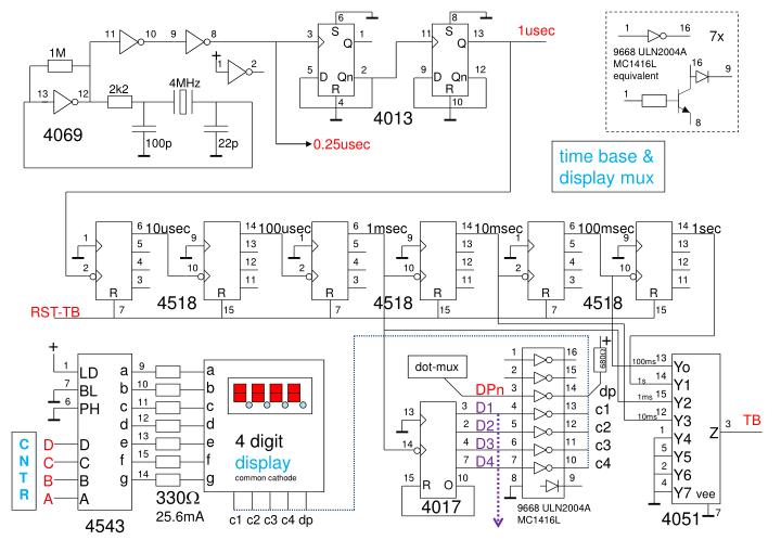
8. 6. 1usec. 1. 16. S. S. 11. 13. 11. 10. 9. 8. 3. 1. 7x. Q. Q. +. 1M. 9668 ULN2004A MC1416L equivalent. 16. 1. 2. 9. 9. 12. 5. 2. D. Qn. D. Qn. 4MHz. R. 2k2. R. 13. 12. 1. 10. 4. 4013. 8. 4069. 100p. 22p. 0.25usec. time base & display mux. 6.

E N D
8 6 1usec 1 16 S S 11 13 11 10 9 8 3 1 7x Q Q + 1M 9668 ULN2004A MC1416L equivalent 16 1 2 9 9 12 5 2 D Qn D Qn 4MHz R 2k2 R 13 12 1 10 4 4013 8 4069 100p 22p 0.25usec time base & display mux 6 10usec 14 100usec 6 1msec 14 10msec 6 100msec 14 1sec 1 9 1 9 1 9 5 13 5 13 5 13 4 12 4 12 4 12 2 10 2 10 2 10 3 11 3 11 3 11 R R R R R R 4518 4518 4518 RST-TB 7 15 7 15 7 15 + + 1 16 13 680W 100ms Yo Y1 Y2 Y3 Y4 Y5 Y6 Y7 1 dot-mux 9 a b c d e f g a b c d e f g LD BL PH D C B A 2 15 14 1s 7 10 DPn D1 D2 D3 D4 3 14 dp c1 c2 c3 c4 15 1ms 6 11 3 4 13 13 12 12 10ms TB 2 5 12 3 1 Z 13 4 digit display common cathode C N T R D C B A 4 6 11 14 5 15 7 7 10 2 14 15 10 8 9 4 R O 330W 25.6mA vee 4017 9668 ULN2004A MC1416L 7 4051 c1 c2 c3 c4 dp 4543
RST CLK 4 12 13 3 4 12 13 3 4 12 13 3 4 12 13 3 11 10 9 P0P1P2P3 P0P1P2P3 P0P1P2P3 P0P1P2P3 A0A1A2 15 1 15 1 15 1 15 1 PL TCn PL TCn PL TCn PL TCn E 7 7 7 7 5 5 5 5 4051 CE BIN/DECn UP/DNn 4029 CE BIN/DECn UP/DNn 4029 CE BIN/DECn UP/DNn 4029 CE BIN/DECn UP/DNn 4029 DP1n DP2n DP3n DP4n 9 9 9 9 13 Y0 Y1 Y2 Y3 Y4 Y5 Y6 Y7 10 10 10 10 + + + 14 + 15 O0O1O2O3 O0O1O2O3 O0O1O2O3 O0O1O2O3 DPn 3 12 Z 6 11 14 2 6 11 14 2 6 11 14 2 6 11 14 2 Counter 1 5 15 1 10 9 15 1 10 9 15 1 10 9 15 1 10 9 2 P0P1P2P3 P0P1P2P3 P0P1P2P3 P0P1P2P3 14 14 14 14 4 R U D PL R U D PL R U D PL R U D PL VEE 5 5 5 5 12 12 12 12 TCu TCd TCu TCd TCu TCd TCu TCd 40193 40193 40193 40193 13 13 13 13 4 4 4 4 + + + + dot-(dp)mux 7 11 11 11 11 4532 O0O1O2O3 O0O1O2O3 O0O1O2O3 O0O1O2O3 5 + E 3 2 6 7 3 2 6 7 3 2 6 7 3 2 6 7 Latch 4 6 I7 I6 I5 I4 I3 I2 I1 I0 O2 O1 O0 3 7 LSB LEn MSB 2 9 1 12 14 15 11 1 5 2 4 12 14 15 11 1 5 2 4 D4 D3 D2 D1 13 Mux 0A1A2A3A 0B1B2B3B 0A1A2A3A 0B1B2B3B 12 6 6 COUNTER E A0 A1 E A0 A1 Eo GS 15 4052 4052 11 10 10 14 10 9 9 ZA ZBVEE ZA ZBVEE 13 3 7 13 3 7 Dec -> Bin B A D C
+ 10kW INPUT clock gate circuit 1usec 9 40175 (CNTR OUT) + 1 R reset & latch circuit 6 8 TB & & & & & & & & & & R-TBS S S TBP 11 13 3 1 Q Q 15 O3 O3n O2 O2n O1 O1n O0 O0n 4013 14 4069 9 12 5 2 D Qn Qn 13 D D3 D2 D1 D0 10 8 R TB1 10 5 6 R 12 11 9 4 10 RSTn RST RST-TB 5 7 TBP 4 4011 6 1 2 TB2 3 12 CLK 2 11 3 5 LEn + 13 4 RST 4011 TB2 6 >10kL,<10kH 6 S RS1 3 1 Q >10kH 13 11 DP1n 2 12 5 Qn D R TBS9 >100kL 5 decimal point decoder & latch 4 DP2n 4 6 >100kH TBS8 8 1 S 11 13 RS0 DP3n >1ML Q 3 2 TBS7 12 >1MH 8 11 9 12 Qn D 10 13 8 R DP4n 9 10 4011 10 9 4013 4011
4013 4013 TBS2 8 8 6 6 6 14 100usec TBS1 S S S S 11 13 11 13 0.25usec 3 1 1 9 1 3 5 13 Q Q Q Q TBS3 4 12 2 10 3 4 9 12 9 12 5 2 2 Qn 5 D Qn D Qn D Qn 3 11 D R R R R R R 4518 4069UB 10 10 4 7 15 4 R-TBS 1up 10up 100up 6 6 6 time base select circuit (frequency detector) S S S 3 1 3 1 3 1 Q Q Q 5 2 5 2 5 2 D Qn D Qn D Qn R R R 4 4 4 4013 4013 4013 TBS4 TBS5 TBS6 8 8 8 S S S >10kL,<10kH 11 13 11 13 11 13 >1ML >100kL Q Q Q 9 12 9 12 9 12 >1MH >100kH >10kH D Qn D Qn D Qn R R R 10 10 10