Download
1 / 37
470 likes | 916 Views
J Morse, Instrument Support and Development Division, European Synchrotron Radiation Facility, Grenoble. Energy Dispersive X-ray Detectors for Spectroscopy Applications. Talk Outline. what are the (synchrotron) requirements?. semiconductor E nergy D ispersive X -ray detectors:

E N D
J Morse, Instrument Support and Development Division, European Synchrotron Radiation Facility, Grenoble. Energy Dispersive X-ray Detectors for Spectroscopy Applications
Talk Outline • what are the (synchrotron) requirements? • semiconductor Energy Dispersive X-ray detectors: principle of operation, material limitations • energy resolution and Fano statistics • preamplifier and electronic noise • signal pulse processing and the pile-up limit • mutielement arrays: the crosstalk challenges • summary
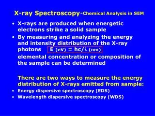
PEAK Energy resolution: many measurements concern identification and quantification of elements in sample. Requirement in this case is to resolve individual K, L, (M) fluorescence lines ‘FWHM’ is the usual figure of merit, typically need ΔE ≤ 200eV. Gaussian line shape is usually assumed (often wrongly) For trace element analysis -- where we may look for ppm levels in a sample matrix that scatters the incoming beam and itself fluoresces — ‘peak-to-valley’ performance of the detector may be of equal importance FWHM 3500 Scattered X rays from incoming X ray beam Sample 3000 X-ray Counts Monochromatic X-ray beam 2500 X-ray counts 2000 Si escape peak from detector 1500 FeKα fluorescence from sample 1000 Energy dispersive detector energy 500 VALLEY 5000 5500 6000 6500 7000 7500 8000 X-ray photon Energy (eV) what are the (detector) requirements ? Energy range: ‘3rd Generation’ Synchrotrons, X-ray photons ~1 keV to >100keV
e.g. for high spatial resolution ‘µ-mapping measurements’: ESRF ID21 Neurite process A Carmona et al JAAS (2008) ESRF ID22NI Counting rates Energy spectra histograms can only be obtained by analyzing individual photon energies on a ‘count by count’ basis At synchrotons, high beam intensities high total spectrum counting rates are required, 103…>106 counts/sec For analysis of chemical states (e.g. SO4n-… XANES, EXAFS studies), higher resolution may be required. In this case, the incoming synchrotron beam energy crystal monochromator is energy scanned with ΔE ~1eV to determine spectral response of sample an energy resolving detector is still required for dilute samples
adequate FWHM resolutions of known lineshape (needed for spectrum deconvolution) 300 ms 300 s Bovine liver ‘thick’(200µm) standard beam normal incidence on sample, Vortex silicon drift detector detector at 75º beam 45 deg incidence, detector at 90º detection limits are set by counting statistics P Cloetens, ESRF-ID22N Count rates and detection limits • For quantitative element analyis, Silicon and Germanium semiconductor detectors are used: • fast photon event count counting in parallel, i.e. over all energies in spectrum • good efficiency possible (solid angle covered by detector)
…but not always! ESRF-ID21 X-ray beam Ω Ω detector sample Sample environment Detector and the beamline environment • Synchrotrons X-ray beams are focused onto sample • emission of sample fluorescence, scatter is from a quasi-point source (~1 …100µ size) • Fluorescence emission is isotropic • ideal detector should cover a 4π solid angle for 100% efficiency size of detector is best defined in terms of its solid angle coverage a small detector close-up can be as effective as a ‘big’ detector further away • Sample environment constraints highly variable: • high pressure (e.g. diamond anvil cell and press) • cryogenic or high temperature furnace (! infra red background) • vacuum • - available space around sample (microscope, other detectors and instruments… other ‘constant’ problems for detector operation: -vibrations – accoustics -electrical interference from other equipment… Electro- Magnetic Compatibility (EMC)
X-ray semiconductor electrical contacts • - photoelectric conversion of an X-ray creates ‘hot’ electrons which rapidly thermalize (~psec), • hole, electron charges drift in applied field towards electrodes • - electrical signal develops while the charge drifts in the bulk Semiconductor detectors: principle of operation Semiconductor material (e.g. crystal of Si or Ge) with X-ray transparent contacts, applied electric field depletes bulk of thermally generated free charge.
not a new idea… “The crystal counter: a new instrument in nuclear physics”, P.J. Van Heerden,PhD Dissertation, Rijksuniversiteit Utrecht, July 1945 • but in practice needed development of • materials in which photoelectric charge is not ‘lost in transit’, i.e. by trapping at crystal structure defects or impurity sites ( Ge(Li), Si(Li)… high purityGe, Si crystals) • development of (surface) electrical contact technologies (problems of time • dependent ‘polarization’ effects, charge injection…)
At ‘low’ energies, photoelectric effect is dominant: µ(E) ~ E 3…4 but µ is discontinuous at ‘absorption edges’ corresponding to atomic shell structure binding energies K, L absorption edges X-Ray absorption in various detector materials Beer’s law: I(x) = Ioexp(-µ(E). x) intensity of a photon beam decreases with distance into material, !! the energy of indvidual photons remains the same. 40µm of Ge (or GaAs) has same total X-ray absorption as ~500µm Si
Useful detector energy range is set by photon absorption range in material (s) • ‘window’ transmission cut-off (detector vacuum • window (K shell fluorescence photon) Ge • transmission loss at higher energies Absorption efficiency loss occurs at binding energies of electrons corresponding to shell levels. This is associated with probability of fluorescence emission ‘Escape’ peaks appear in detector energy spectrum at energies (EXray- Efluo), where Efluo transition energy for electron falling from L, M… levels to inner K shell energy level e.g. for Ge Efluo ≈ 9.9 keV (Kα), 1.2 (Lα1) for Si ≈ 1.74 (Kα) Escapes complicates spectra with multiple peaks, and information may be ‘lost’ by peak overlaps photoelectron Material absorption effects on energy spectrum • inefficient charge collection for absorption close • to front contact of semiconductor - incomplete energy absorption (loss by Compton Scattering)
Detector Material photoelectric absorption Compton scattered photon escapes detector √ all incident photon energy measured (recoil electron + Compton photon) X measured energy = Compton recoil electron only Compton Scattering and energy loss E = hc/ λ
Fano energy resolution, leakage current (noise) Signal development time (max. counting rate) stopping power, X-ray absorption length monoelemental crystals, excellent charge transport 4500 3500 • Binary and ternary compounds • Stochiometry etc • trapping of charge during drift (signal loss) Semiconductor materials for γ and X-ray detection
Lower bandgap materials can offer better resolution due to better Fano statistics NQ is number of generated charge carriers, F is ‘Fano factor’ Cooling below room temperature needed But low bandgap materials must be cooled to limit noise from thermal generation of carriers ~exp( /kT) and often suffer from ‘charge trapping’ statistics and energy resolution Absorbed radiation energy E is shared between crystal lattice excitations (~2/3) and generation of charge carriers(~1/3) this ratio is ~same for many semiconductor materials
Recall, ultimate ‘theoretical’ energy limit set by Fano statistics: FWHM = 2.35√FεEε =3.63 eV/e-h for Si Fano factorF≈ 0.11 for Si and Ge (F is not a constant) U. Fano, Phys. Rev. 72 (1947) 26 MnKα (Fe55 source) But measured spectral resolution R is quadrature-sum of above Fano statistics and electronic noise : R = √ (Fano)2 + (electronic noise)2 • R should have ~Gaussian symmetric shape, but rarely does at ≤ 1% level… multiple causes: • near surface X-ray absorptions with • incomplete charge collection • ‘ballistic deficit’ associated with charge • collection and pulse filtering time • pulse processor effects (pile-up and baseline • degradation at high count rates) Peak-valley performance may be critical energy resolution and electronic noise
Silicon detector, 300µm thick, Vdepletion= 60V, Vbias= 200V T= 300ºK Vbias Vbias - - + + X-ray photoelectric absorption: High energy physics: MIP particle track different interaction depths for each photon x assuming no charge trapping! Signal: time development for photons variation in signal-time development according to photon interaction point In spectroscopy measurements, problem is avoided by use of charge sensitive preamplifier which integrates the i(xabsorption, t) signal current
Pulse restore preamp RP Signal amplitude ID Cf gm C semiconductor FET-charge preamp crystal time Signal output from preamplifier charge preamp, signal out (volts) = charge in (from X-ray photo-conversion) preamp feedback capacitance Cf the charge preamplifier Charge preamplifier Signal amplitude is proportional to collected photoelectric charge (i.e. to X-ray energy) …and independent of detector bias, interaction point (charge drift time variations)
preamplifier noise: theory Charge q created by X-ray absorption is q = 1.6 x 10⁻¹⁹ Exray(eV)/ (Coulombs) = 3.63eV / electron-hole pair for Si , 2.9eV / electron-hole pair for Ge For charge preamplifier, ‘Equivalent Noise Charge’ (expressed in e- r.m.s)analysis gives total noise parallel noise series noise 1/f noise ‘parallel’ ‘series’ τis signal ‘shaping time’ for germanium detector preamp’ with typical feedback Cf=0.1pF, a 10keV Xray gives a voltage step signal of only 0.5mV and we need to measure this with a precision of <1% ! NOISE contribution of electronics (preamplifier) must be minimized
silicon detector array, LBL Detetctor cooling -minimize detector ‘leakage current’ ID reduce temperature, detector material bulk and surface, design tricks C reducing -minimize C (crystal geometry, ‘drift diode’ designs, FET type/integration) noise: practice To reduce noise: -maximize RP OK, RP ∞ by using a ‘pulse restore’ -minimize kT (OK, cool detector, but limits to this…) -optimize choice of τ pulse shaping (or peaking) time can be varied ‘online’ as needed by experiment… …but need to count at high rates (≥ 1/10τ)limits the maximum τ values, i.e. problems of pulse pile-up…
Pulse processor (for spectroscopy, now almost always ‘digital’ systems) has several tasks: minimize preamp noise contribution to resolution (filter peaking time and shape ) detect and reject pulse pile-up events (and detector preamp pulse restores…) and record corresponding detector ‘dead time’: X-ray events Fast channel (time info’) PUR peaking time ‘slow’ channel (energy) spectrum signal pulse processing
TP TP time between pulses increasing TP For Poisson time-distributed X-ray events, measured spectrum output count rate can be obtained from ICR = OCR exp(-ICR xTP) TP≈5x pulse ‘shaping time’ or ≈ 2x ‘peaking time’ OCR = ICR OCR dead time losses Limits to OCR usually: Low counting rates: insufficient detector size (solid angle) High counting rates: TP cannot be reduced (energy resolution degrades!) multielement detector systems TP ICR=OCR/ TP(1-OCR) 1/eTP ICR = OCR exp(-ICR x TP) ICR 1/ TP signal pulse ‘pile-up’ Spectroscopy pulse processors are ‘paralysable’: -‘dead-time’ TP for processing each event - any second event coccurring within time TP must be rejected to avoid false ‘pileup’ peak in spectrum
SDDs exploit the complex processing technologies available for planar processing of silicon: multielectrodes establish transverse drift field charge collected over large surface area (≤1cm2) without increasing anode capacity X ray X-rays silicon drift diode (SDD) Charge carriers collected by low capacity anode electrode contact preamp’ first stage may be integrated into detector (C <100fF) • high resistivity (i.e. low impurity) silicon low bulk leakage current • thermoelectric Peltier cooling -10ºC…-70ºC is sufficient for spectroscopy with • pulse processor peaking times ~0.2 … ~10 µsec • compact and lightweight (~kgm) systems, insensitive to accoustics-vibrations
SDD: a very clever trick Gatti et al. IEEE Trans. Nucl. Sci. NS-32 (1985) 1204)
ESRF ID22NI ~ 200mm P/V Throughput count rates to ~500kcps possible (0.25µs peaking, 230eV MnK FWHM ) cf. Si(Li) detector ~25kcps (5µs peaking 160eV MnK FWHM) X-ray beam 5000 20000 0 sample 10000 15000 but peak / valley 700 ~1000 cf. 10 000 for Schottky Si(Li) or Schottky Ge practical SDD detector for high count rates SII ‘Vortex’ drift diode discrete JFET preamp with pulse restore operation no energy peak shifts with counting rate ~47mm2 active detection area test data (Mn foil fluo’), ID21 ESRF
~ 20mm grid supported ultrathin (~0.5µ) polymer window data from pndetector.de (2µS pulse processor peaking time) Peltier thermoelectric cooler -20ºC SDDs with higher peak-valley performance - very shallow, abrupt dopant-profile implant for front contact - Zr collimator ring (avoids partial charge collection from X-rays at detector periphery
Collimating mask e.g. Zr FET • + metal collimator • peak / valley of 7000 • radiation protection of FET (hole-accumulation in surface oxide and trapping at Si- SiO2 interface) teardrop SDD standard SDD peripheralevents events near FET ‘teardrop’ SDD design integrated FET structure near Fano-limited resolution at low count rates (peaking times >1µs) pnSensor GmbH teardrop geometry but SDD Si thickness limit ~0.4mm cf. 3mm for ‘conventional’ Si(Li) structure and >10mm for Ge
multielement detectors and beam polarization Multielement detectors can offer higher overall count rates: e.g. for N independent counting channels and uniform angular distribution of counts we can expect a total count rate capability increased N-fold multielement detectors (e.g. germanium 13 – 100 elements) are now commercialized • Synchrotron undulator beams focused on sample are typically ~ 99% linear polarized • angular dependence of both Rayleigh (elastic) Compton (inelastic) scattering • but an EDX detector measures total count rate (i.e. fluorescence and scatter) • in practice, effective count rate gain from an N channel detector is <N or <<N, and dependent on: - the experiment-detector geometry - the sample under investigation (concentration, matrix Z, crystallinity…) - energy of excitation beam
non isotropic process • Cross section for fluorescence radiation is isotropic (independent of ) Scattering of linear polarized radiation Polarization dependentelastic scattering cross section: Compton scattering ignored here (‘low energy’ case) R. E. van Grieken, A. A. Markowicz, Handbook of X-ray Spectrometry (2002). max horizontally polarized x-ray beam min max min max max
central element of multiement detector Photon density distributions projected on central element of detector Sample Elastic scatter Fluorescence 20mm 30mm 20mm Spectrum recorded by central element Fe in low-Z matrix Monte-Carlo calculations: L. Vincze et al., Spectrochimca Acta B, 48, 553 (1993), 50, 127 and 1481 (1995), 54 1711 (1999).
Elastic scatter 8 8 19 9 19 9 Sample 18 18 2 2 10 10 7 7 3 3 17 17 11 11 1 1 4 4 6 6 16 16 12 12 5 5 20mm 30mm 15 15 13 13 14 14 20mm importance of multielement ‘packing factor’ i.e. inter-element dead spaces Ideal case 8 19 9 18 2 10 7 3 17 11 1 usual case for ‘discrete elements’ 4 6 16 12 5 15 13 Si escape 14 detection limit with multielements Application: fluorescence from ‘dilute’ samples J Slazchetko, ESRF
After an X-ray is absorbed, diffusion creates a ‘cloud’ of electric charge which may be split the signal between bordering sensing areas. As well as its shunt capacity to a common rear electrode contact, each sensing area is capacitively coupled to its neighbours. Electronic crosstalk from individual fet preamplifier restore switching generates false spectral peaks. Problem is worst for short pulse processor peaking times. Solution is ‘synchronous’ FET restore or signal veto. monolithic multielement detectors a semiconductor can be electrically segmented by lithographic mask doping of contacts to create an x, y matrix of individual sensing areas. This gives a 100% sensitive area but there are problems: Alternatively, a fluorescence photon may be emitted and absorbed in a neighbour sensing area These physical crosstalk effects clearly become more serious as the individual detector areas are reduced in size. Solution is use of a grid collimator covering border areas.
Molybdenum mask on planar silicon detector developed at NSLS-BNL 384 detector elements each 1 mm2 area, 400µm thick n-type silicon Mo mask, peak-valley 1000 C.G. Ryan et al. /Nucl. Instr. and Meth. Phys. B 260 (2007) 1–7 No mask peak-valley 200 multielement detectors: use of collimator mask
monolithic multielement devices multielement silicon drift diode arrays ‘near wafer-scale’ lithographic processing large, tightly-packed arrays possible 39 cell detector with on-chip FETs, total active area 195mm2 (after L Strüder, MPI-Garching) other practical challenges of large cell counts: yield issues (bad cell and cell-to-cell variability, especially on-chip FET parameters) power dissipation (cooling!) need for multi channel pulse processors overall system fabrication complexity / cost
Compton profiles Compton scattered photon peak elastic scattered photon peak (beam energy) high energy spectroscopy at ESRF magnetic Compton scattering spectra (fixed, monochromatic beam energy ~50 … 150keV) Slit selection of Compton backscatter angle sample monochromatic beam Ge detector At present, only Germanium detectors are adequate for this application: - high Z for adequate absorption (large detector volumes (>cm3) with negligible charge carrier trapping) -high energy resolution (ΔE/E ~0.5% at 100keV) and clean Gaussian line shape
Spatial resolution ~0.1x0.1mm2 Ge detector diffraction peak intensity (counts) Ehkl d sinθ =hc / 2 Bragg’s Law ESRF ID15 Energy (keV) high energy spectroscopy Strain scanning of materials with white beam (E ~100…250keV) e.g. Ti-alloy aircraft turbofan blade sample is stressed in-situ shifts in diffraction peak energies give Δd strain values, or fixed strain patterns in a sample may be mapped by x, y scanning in the beam Two detectors give simultaneous measurements in orthogonal scattering planes strain tensor measurement
Φ= 5 cm, L = 7 cm ‘Clover’ detectors shaped for close-packed geometry and near 4π solid angles in nuclear pyhsics experiments eurogam2 P. Jones et al., Nucl. Instr. and Meth. A 362 (1995) 556 Detectors can also be electrically ‘segmented’ to give better tracking granularity even higher energies (> MeV…) • At high energies, Compton scattering is dominant interaction • large volume Germanium detectors required • spectroscopy possible by reconstructing photon interactions using information from multiple detectors • partially absorbed events can be vetoed
Summary At low count rates (<< 1/peaking time) Silicon and Germanium approach theoretical performance limits (Fano statistics) over the large range of X-ray energies used at 3rd generation synchrotrons. Higher ΔE/E resolutions or better X-ray absorption may be theoretically be obtained with compound semiconductor materials. For precise, quantitative spectroscopy, there are no competitors to Siilicon and Germanium due to lack of large, pure, and perfect crystals of binary or ternary compounds. For low energies (>20keV), Silicon is a near-ideal detector material offering advanced processing technologies including the fabrication of on-detector low-noise electronics. Higher energies require Germanium, but detectors made from this material are unlikely to ever reach the sophistication of silicon devices due to the lack of a large scale market (i.e. electronics) to support the needed developments. Pulse processor pile-up effects degrade spectral quality and counting efficiency at high count rates (≥ 1/peaking time). Multi-element detectors may attain higher count rates but the gain is limited by geometric considerations and the practical challenges of making individual detector channels operate in a truly independent manner.
some bibliography Radiation Detectors in general: G Knoll ‘Radiation Detection and Measurement’, Wiley , 2000 C Delaney, E Finch ‘Radiation Detectors: Physical Principles and Applications’, OUP 1992 Semiconductor Detectors, detailed physics: H Spieler, ‘Semiconductor Detector Systems’, OUP, 2005 G Lutz, ‘Semiconductor Radiation Detectors: Device Physics’, Springer Berlin 1999 EDX detectors, application issues (n.b. mainly for analytical electron microscopy): J Goldstein et al, ‘Scanning Electron Microscopy and X-Ray Microanalysis’, Springer 2003 R Van Grieken et al, Handbook of X-Ray Spectrometry, Dekker 2002