Download
1 / 28
280 likes | 429 Views
ZENO EFFECT, RIDGED MIRRORS and ATOMIC NANOSCOPY. Dmitrii Kouznetsov, Inst. for Laser Science, UEC. To. Collaboration: Hilmar Oberst, Fujio Shimizu, Kazuko Shimizu, Makoto Morinaga, Junichi Fujita, J-F. Bisson, Kenichi Ueda (Japan); and

E N D
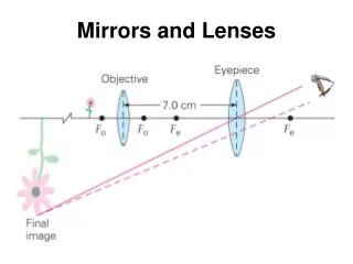
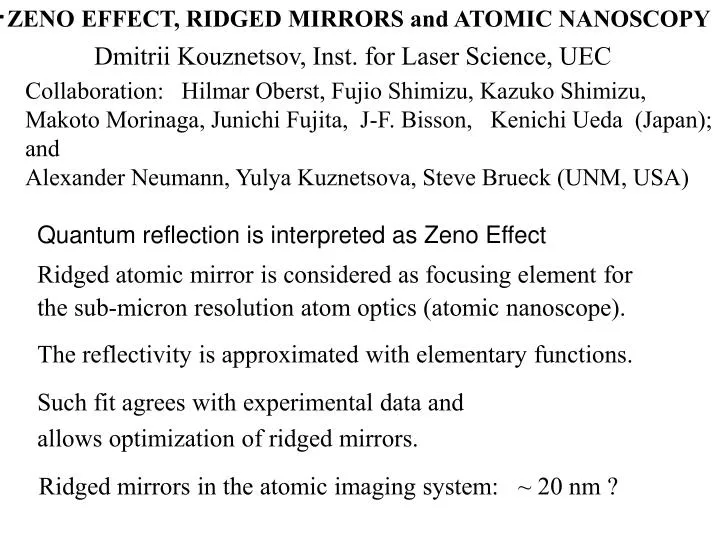
ZENO EFFECT, RIDGED MIRRORS and ATOMIC NANOSCOPY Dmitrii Kouznetsov, Inst. for Laser Science, UEC To Collaboration: Hilmar Oberst, Fujio Shimizu, Kazuko Shimizu, Makoto Morinaga, Junichi Fujita, J-F. Bisson, Kenichi Ueda (Japan); and Alexander Neumann, Yulya Kuznetsova, Steve Brueck (UNM, USA) Quantum reflection is interpreted as Zeno Effect Ridged atomic mirror is considered as focusing element for the sub-micron resolution atom optics (atomic nanoscope). The reflectivity is approximated with elementary functions. Such fit agrees with experimental data and allows optimization of ridged mirrors. Ridged mirrors in the atomic imaging system: ~ 20 nm ?
Collaboration: Hilmar Oberst, 清水 和子, 清水 富士夫, 藤田 淳一, J-F.Bisson, 植田 憲一 (日本); and A.Neumann, Yu.Kuznetsova, S.R.J.Brueck (UNM, USA) K. Ueda Fujio Shimizu collaboration with Kazuko Shimizu 清水 富士夫 清水 和子, Hilmar Oberst JF Bisson 植田 憲一 pics Makoto Morinaga Center for High Technology Materials, UNM, USA J. Fujita 藤田 淳一 Steve Brueck Yu.Kuznetsova A. Neumann
原子スキー ATOMICSTAFF ATOMIC BOMB ATOMIC SKI ATOMIC CLOCK ATOMIC PLANT ATOMIC FORCE げんしどけい げんしりょく はつでんしょ げんしりょく
More atomic staff atomic mirror P.Bertram, H.Merimeche, M.M\"utzel, H.Metcalf, D.Haubrich, D.Meschede, P.Rosenbusch, E.A.Hinds. Magnetic whispering-gallery mirror for atoms. PRA 63, 053405 (2001) Ashok Mohapatra. The same for the normal incidence. (reported here yesterday, 2007) atomic Fresnel zone plate Bruce Doak et al. Towards realization of an atomic de Broglie microscope: helium atom focusing using Fresnel zone plates. PRL 83, p.4230-4232 (1999) atomic lens V. Balykin, V. Klimov, V. Letokhov. Atom nano-optics. Opt. and Phot. News 16, 44 (2005)
What is QUANTUM REFLECTION? Wikipedia: Quantum reflection is a classically counterintuitive phenomenon whereby the motion of particles is reverted "against the force“ acting on them. How about reflection of solitons? Andy Martin. Quantum reflection of solitons and bright solitary waves. Ilya Dodin (Classical analogies of atom manipulation Techniques using laser radiation) also doubts if that he does is Quantum reflection. Perhaps, any counter-intuitive reflection should be called so.
Should we call “quantum reflection” any scattering of any wave at any structure? Reflection of oceanic waves from a periodic groin field, is it also quantum reflection?
The Zeno effect is Class of phenomena when a transition is suppressed by interaction which allows the interpretation of the final state in terms transition has not yet occurred or transition already occurred. Z In quantum mechanics, such an interaction is called measurement; its result can be interpreted in terms of classical mechanics. Frequent measurement prohibits the transition. We apply the concept of the Zeno effect to the transition of the atom from the half-space y>0 to the half-space y<0 . Ridges appear as a device that measures, whether the atom already collided with the mirror or not yet. y - position is periodically measured. rate of measurement frequent measurement prohibits the transition.
Most of our results are published. D.Kouznetsov, H.Oberst. Reflection of waves from a ridged surface and the Zeno effect. Opt.Rev. 12, p.363-366. (2005) http://www.ils.uec.ac.jp/dima/PAPERS/optrevri.pdf D.Kouznetsov, H.Oberst. Scattering of atomic matter waves from ridged surfaces. PRA 72, 013617 (2005) http://www.ils.uec.ac.jp/~dima/PAPERS/PhysRevA_72_013617.pdf H.Oberst, D.Kouznetsov, K.Shimizu, J.Fujita, F.Shimizu. Fresnel diffraction mirror for an atomic wave. PRL 94, 013203 (2005). http://www.ils.uec.ac.jp/~dima/PAPERS/PhysRevLett_94_013203.pdf D.Kouznetsov, H.Oberst, A.Neumann, Y.Kuznetsova, K.Shimizu, J.-F.Bisson, K.Ueda, S.R.J.Brueck. Ridged atomic mirrors and atomic nanoscope. J.of Physics B 39, p.1605-1623 (2006) http://stacks.iop.org/0953-4075/39/1605 http://www.ils.uec.ac.jp/~dima/PAPERS/nanoscope.pdf Di
R.Poelsema. G. Comsa. Scattering of thermal energy atoms from disordered surfaces. (Springer-Verlag, 1989) The method based on the thermal energy atom scattering (TEAS), that we are reviewing here, appears to complement in an ideal way scanning tunnel microscopy in the investigation of disordered surfaces. quotes: B.Holst, W.Allison. An atom-focusing mirror. Nature, v.390, p.244 (1997). (He atoms, wavelength 0.52 A, spot diameter 210 micron): It follows that a helium microscope with nanometer resolution is possible. A helium atom microscope will be unique non-destructive tool for reflection of transmission microscopy. What is optimal design for the focusing element? F.Shimizu, J.Fujita. Giant Quantum Reflection of Neon Atoms from a Ridged Silicon Surface. J.Phys.Soc. of Japan 71, p.5-8 (2002): The specular reflectivity of slow, metastable neon atoms from a silicon surface was found to increase markedly when the surface was replaced by a grating structure with parallel narrow ridges. The reflectivity was found to increase more than two orders of magnitude at the incident (grazing) angle 10 mrad. Further improvement of the reflectivity at a larger angle will be possible if the width of the ridge and the periodicity are reduced. What is optimal periodicity at given width? How far can be extended the working range of the grazing angle? What resolution of the atom optics imaging system does it correspond?
potential 4 U( y ) = C / y 4 flat mirror Depth: From the dimensional reasons, the reflectivity of a flat atomic mirror should be determined by Fit: k = K s H.Oberst, Y.Tashiro, K.Shimizu, F.Shimizu. Quantum reflection of He* on silicon. PRA, 71, 052901 (2005) F.Shimizu. Specular reflection of very slow metastable neon atoms from a solid surface, PRL 86, 987-990 (2001). Interaction is described with Hermitian potential
RH F.Shimizu, J.Fujita. Giant quantum reflection of Ne atoms from a ridged silicon surface J.Phys.Soc. of Japan, 71, p.5-8 (2002) H.Oberst, D.Kouznetsov, K.Shimizu, J.Fujita, F.Shimizu. Fresnel diffraction mirror for an atomic wave. PRL 94, 013203 (2005)
estimate the reflectivity of a ridged mirror? Estimate of reflectivity of ridged mirrors with scaling of the van der Waals constant: lg(R) Ne* atoms, V=3m/s F.Shimizu, J.Fujita. Giant Quantum Reflection of Neon Atoms from a Ridged Silicon Surface J.Phys.Soc. of Japan 71, p.5-8 (2002):
B. Mielnik. The screen problem. Foundatons of Phys., 24, p.1113-1129 (1994): “…interpretation of the quantum mechanical wave packet contains a gap.” Can we reflect an object by the intensive observation in a half-space? SP detectors normal component of velocity frequency of measurement k = K normal component of wavevector ridged mirror
Continuous absorption with rate f = V/L also causes reflection C
AGREEM R Reflectivity can be estimated as photons 0.1 This estimate ignores width of the ridges and the van der Waals interaction, but agrees with experimental data. 0.01 Hilmar: Incredible coincidence!
Some colleagues were not satisfied with the deduction. The numerical analysis for the idealized ridges can be summarized with fit II Such fit overestimates the reflectivity. (PRA,2005) perturbative correction suggests to reduce L to improve the reflection… UNM sample
properties of R(,,,,) at large L , small s ,
Scaling of VWI: Fits Zeno - optical fit (large L ) Perturbative Combined a=1/4 , b=3 , c=4 holds in wide range of parameters
Projection of reflectivity pqA to the p, q plane 4 0 0 < ーLn R < 1 11 < ーLn R < 2 22 < ーLn R < 3 33 < ーLn R < 4 4 4 < ーLn R < 5 55 < ーLn R < 6 66 < ーLn R < 7 77 < ーLn R < 8 3 2 1 all experimental data collected 1 2
q q pq ーLn R ーLn R , experiment ーLn R , fit 3 2 1 p p 1 2 1 2
Contour of in the L , plane contour K = 6.3/nm , s = 0.005 , w = 317 nm (He atoms at V=100m/s dashed: in vicinity of optimalL , 0.01 R 0.1 0.2 0.3 0.4
There is optimal period at given width of ridges Hefit w = 317 nm , V = 100 m/s , s = 0.005 , K=6.3/nm (He, T=1K) R 5 = L, micron
V=100 m/s gives 4.8 Kelvin nanoscope concentration Pinhole a=100nm, b=1000nm flux small portion reached the focusing element: atoms/second geom.optics, spotsize: Focusing element wave optics: resulting spotsize:
of Atomic Nanoscope COMPETITORS optical microscopy (also scanning confocal, and near-field ) electron microscopy (including SEM) probe microscopy: atomic force microscopy electrostatic force microscope magnetic force microscopy scanning capacitance microscopy (Kelvin probe) scanning gate microscopy (also tunneling microscopy) scanning thermal microscopy scanning voltage microscopy (maping of the electric potential) also provide the submicron resolution
CONCLUSIUONS 1 p END R .1 R z .01 けつろん q Estimate for reflectivity: -ln R 1 optimal L at given : R=0.1 1nm 0 p 1 0 0.3 1/2 3/4 1/4 R ~ exp( - 2 w K ) 1nm L Nanoscope: For He at V=100m/s (T = 1 K), s = 0.005, = 10 nm, R 0.1 limit of resolution of the atom optical imaging system at 20 nm
Atom optics. B. Poelsema, G. Comsa. Scattering of thermal energy atoms from disordered surfaces. (Springer-Verlag, 1989) J. J. Berkhout et al. Quantum reflection: Focusing of hydrogen atoms with a concave mirror. PRL 63, 1689-1692 (1989) M. Kasevich, D. Weiss, S. Chu. Normal-incidence reflection of slow atoms from an optical evanescent wave. Opt.Lett. 15, 607-9 (1990) E. Hulpke. Helium atom scattering from surfaces. (Springer-Verlag, 1992) D. C. Lau et al. Magnetic mirrors with micron-scale periodicities for slowly moving neutral atoms. J. of Optics B, 371-377 (1999) R. B. Doak et al. Towards Realization of an Atomic deBroglie Microscope: Helium Atom Focusing using Fresnel Zone Plates. PRL 83 , 4229-4232 (1999) D.A.MacLaren, W.Allison. Single crystal optic elements for helium atom microscopy. Rev. of Sci. Instr. 71, p.2625-2634 (2000) M. Drndic et al. Properties of microelectromagnet mirrors as reflectors of cold Rb atoms. PRA 60, 4012 (1999) C. Eltschka, M. J. Moritz, H. Friedrich, Near-threshold quantization and scattering for deep potentials with attractive wells, J. of Physics B 33, 4033-4051 (2000) R. P. Bertram et al.. Magnetic whispering-gallery mirror for atoms. PRA 63, 053405 (2001) A. Pasquini, Y. Shin, C. Sanner, M. Saba, A. Schirotzek, D. E. Pritchard, W. Ketterle. Quantum Reflection from a Solid Surface at Normal Incidence. PRL 93, 223201 (2004) V, Balykin, V. Klimov,V. Letokhov. Atom nano-optics. Opt. and Phot. News 16, 44 (2005) N.P.Robins, A.K.Morrison, J.J.Hope, J.D.Close. Limits to the flux of a continuous atom laser. PRA 72 031606 (2005) po
B.Poelsema, G.Comsa. Scattering of thermal energy atoms from disordered surfaces. (Springer-Verlag, 1989) E. Hulpke. Helium atom scattering from surfaces}. (Springer-Verlag, 1992) V,Balykin, V. Klimov., V. Letokhov. Atom nano-optics, Opt. and Phot. News 16, 44 (2005) M. Kasevich, D. Weiss, S. Chu. Normal-incidence reflection of slow atoms from an optical evanescent wave. Opt. Lett. 15, 607-9 (1990) H. Oberst, S. Kasashima, V. I. Balykin, F. Shimizu. Atomic-matter-wave scanner. PRA 68, 013606 (2003) C. V. Saba, P. A. Barto Boshier, n, M. G. I. G. Hughes, P. Rosenbusch, B.E.Sauer, E.A.Hinds. Reconstruction of a Cold Atom Cloud by Magnetic Focusing. PRL 82, 468 (1999). D. C. Lau et al. Magnetic mirrors with micron-scale periodicities for slowly moving neutral atoms. J. of Optics B, 371-377 (1999) M. Drndic,et al. Properties of microelectromagnet mirrors as reflectors of cold Rb atoms. PRA 60, 4012 (1999) R. P. Bertram, et al.. Magnetic whispering-gallery mirror for atoms. PRA 63, 053405 (2001) J.J.Berkhout et al. Quantum reflection: Focusing of hydrogen atoms with a concave mirror. PRL. 63, 1689-1692 (1989) R.B.Doak et al. Towards Realization of an Atomic deBroglie Microscope: Helium Atom Focusing using Fresnel Zone Plates. PRL 83 , 4229-4232 (1999). F.Shimizu, J.Fujita. Reflection-type hologram for atoms. PRL 88, 123201 (2002) H. Oberst, S. Kasashima, V. I. Balykin, F. Shimizu, Atomic-matter-wave scanner. PRA 68, 013606 (2003) T. A. Pasquini, Y. Shin, C. Sanner, M. Saba, A. Schirotzek, D. E. Pritchard, W. Ketterle. Quantum Reflection from a Solid Surface at Normal Incidence. PRL 93, 223201 (2004) Specular reflection of very slow metastable neon atoms from a solid surface. PRL. 86, 987-990 (2001). H.Oberst, Y. Tashiro, K. Shimizu, F. Shimizu. Quantum reflection of He* on silicon. PRA 71, 052901 %(2005) %[18] ¥bibitem{shim03} Shimizu F and Fujita J 2003 Giant quantum reflection of neon atoms from a ridged silicon surface, {¥em J. Phys. Soc. Jpn.} ¥textbf{71} 5-8 %[19] ¥bibitem{ober05} Oberst H, Kouznetsov D, Shimizu K, Fujita J and Shimizu F 2005 Fresnel diffraction mirror for an atomic wave. {¥em Phys. Rev. Lett.} ¥textbf{94} 013203 %H. Oberst, D. Kouznetsov, K. Shimizu, J. Fujita and F. Shimizu, %Fresnel diffraction mirror for an atomic wave. % Phys. Rev. Lett. ¥textbf{94}, 013203 (2005). %[20] ¥bibitem{zeno05} Kouznetsov D and Oberst H. 2005 Reflection of waves from a ridged surface and the Zeno effect {¥em Optical Review} {¥bf 12} 363-6. %{¥em Optical Review}, 2005, v.12, No.5, p.363-366. % http://www.ils.uec.ac.jp/~dima/optrevri.pdf (99k) %[21] ¥bibitem{kouz05} Kouznetsov D and Oberst H 2005 Scattering of atomic matter waves from ridged surfaces {¥em Phys. Rev.} A {¥bf 72}, 013617 %%[22] %¥bibitem{oberamo06} %Oberst H, Kouznetsov D, Shimizu K, Shimizu F. %2006 %Giant quantum reflection of Ne* on silicon surface structure, %{¥em International Seminar on Progress and Excitement in AMO Physics, %17-18 January, Abstract book} 35 %[23] ¥bibitem{bruc99} Bruce N C, Garc¥'{¥i}a-Valenzuela A and Kouznetsov D 1999 Rough-surface capacitor: approximations of the capacitance with elementary functions. {¥em J. of Phys.} D. {¥bf 32} 2692-702 % N. C. Bruce, A. Garc誕-Valenzuela, D. Kouznetsov. Rough-surface capacitor: approximations of the capacitance with elementary functions. %-- Journal of Physics. D. (Applied Physics), v.32 No.20 (Oct. 21 1999) p.2692-702. %[24] ¥bibitem{elts00} Eltschka C, Moritz M J and Friedrich H 2000 Near-threshold quantization and scattering for deep potentials with attractive wells, {¥em J. of Phys.} B {¥bf 33} 4033-51 %C. Eltschka, M. J. Moritz, H. Friedrich, %Near-threshold quantization and scattering for deep potentials with attractive wells, %Journal of Physics B, {¥bf 33} 4033-4051 (2000) %[24] ¥bibitem{frie02} %Harald Friedrich,* Georg Jacoby, and Carlo G. Meister Friedrich H, Jacoby G, and Meister C G 2002 Quantum reflection by Casimirツュvan der Waals potential tails {¥em Phys. Rev.} {¥bf A 65} 032902 %PHYSICAL REVIEW A, VOLUME 65, 032902 %sik-Department, Technische Universitat Munchen, 85747 Garching, Germany %¥bibitem{ober06} %H. Oberst, J. Fujita, D. Kouznetsov, K. Shimizu, F. Shimizu. %Atom optics using solid surfaces and surface structures. %-- To be published. Abramowitz M and Stegun I A, eds. Handbook of Mathematical Functions, % with Formulas, Graphs, and Mathematical Tables. New York: Dover, 1972. %[26] ¥bibitem{zhan94} Zhang W and Walls D F 1994 Phonon-induced quantum pair correlation in the diffraction of an ultracold atomic beam by a crystalline solid surface, Phys.Rev. {¥bf A} {¥bf50} 4069-76 % 4069-4076 (1994) %[27] ¥bibitem{logo99} Logofatu P C, Coulombe S A, Minhas B K and McNeil J R 1999 Identity of the cross-reflection coefficients for symmetric surface-relief grating {¥em J. Opt. Soc. Am.} ¥textbf{A 16} 1108-14 %P. C. Logofatu, S. A. Coulombe, B. K. Minhas, J. R. McNeil, %%P. C. Logof{a}tu, S. A.Coulombe, B.K.Minhas, J.R.McNeil. %Identity of the cross-reflection coefficients %for symmetric surface-relief grating %J. Opt. Soc. Am. ¥textbf{A 15}, 1108-1114 (1999) %[28] ¥bibitem{gomb04} %Andreas Gombert1, Christopher Buhler1, Wolfgang Hoテ歿eld1, Gombert A, Buhler C, Ho$¥beta$feld W, %Jorg Mick1 , Benedikt Blasi1, Gunther Walze1 and Peter Nitz1 Mick J, Blasi B, Walze G and Nitz P 2004 A rigorous study of diffraction effects on the transmission of linear dielectric micro-reflector arrays. {¥em J. Opt. A: Pure Appl. Opt.} {¥bf 6} 952-60 %begin STRUCTURES %[29] ¥bibitem{chu93} Chu A S, Zaidi S H and Brueck S R J 1993 Fabrication and Raman-scattering studies of one-dimensional nanometer structures in (110) silicon {¥em Appl. Phys. Lett.} {¥bf 63} 905-7 %A. S. Chu, S. H. Zaidi, S. R. J. Brueck. Fabrication and Raman-scattering studies of one-dimensional nanometer structures in (110) %silicon. Appl. Phys. Lett., {¥bf 63} 905-907 (1993) %no.7, p.905-907 %[30] ¥bibitem{wang05} %Jian Jim Wang,a Feng Liu, Xuegong Deng, Xiaoming Liu, Lei Chen, Wang J J, Liu F, Deng X, Liu X, Chen L, %Paul Sciortino, and Ron Varghese Sciortino P and Varghese R 2005 Monolithically integrated circular polarizers with two-layer nano-gratings fabricated by imprint lithography {¥em J. Vac. Sci. Technol.} {¥bf B 23} 3164-7. %end STRUCTURES %begin WIRES %[31] ¥bibitem{weis02} %Peter Weiss Weiss P 2002 Circuitry in a nanowire: Novel growth method may transform chips %Week of Feb. 9, 2002; Vol. 161, No. 6 , p. 83 %Science News, Vol. 161, No. 6, Feb. 9, 2002, p. 83. {¥em Science News} {¥bf 161} 83 %[32] ¥bibitem{lee04} Lee S C and Brueck S R J 2004 Nanoscale two-positional patterning on Si(001) by large-area interferometric lithography and anisotropic wet etching. {¥em J. Vac. Technol.}{¥bf B 22} 1949-52 %S. C. Lee and S. R. J. Brueck. %Nanoscale two-positional patterning on Si(001) by large-area interferometric lithography and anisotropic wet etching. %J. Vac. Technol.{¥bf B 22}, 1949-1952 (2004) %[33] ¥bibitem{ding05} %Remi Dingrevillea, Jianmin Qua, , Mohammed Cherkaouib Dingrevillea R, Qua J, Cherkaouib M 2005 Surface free energy and its effect on the elastic behavior of nano-sized particles, wires and films {¥em J. of the Mechanics and Physics of Solids} % 53 (2005) 1827ツュ1854 {¥bf 53} 1827-854 %end WIRES %begin EXTRA REFERENCES %¥bibitem{ress92} %Ress D, Lerche R A and DaSilva L 1992 %Demonstration of an x-ray ring-aperture microscope for inertial-confinement fusion experiments %{¥em Appl. Phys. Lett.} {¥bf 60} 410-2 %%(4), 27 January %%%D. Ress, R. A. Lerche, and L. Da Silva. %%Demonstration of an x-ray ring-aperture microscope for inertiai-%confinement fusion experiments. %Appl. Phys. %Lett. {¥bf 60}410-412 (1992) %(4), 27 January %¥bibitem{robi05} %Robins N P, Morrison A K, Hope J J and Close J D 2005 %Limits to the flux of a continuous atom laser. %{¥em Phys. Rev.} A {¥bf 72} 031606 %%N. P. Robins, A. K. Morrison, J. J. Hope, and J. D. Close. %%Limits to the flux of a continuous atom laser. %%Phys. Rev. A {¥bf 72} 031606 (2005) %end EXTRA REFERENCES several papers are written by my co-authors: F.Shimizu. Specular reflection of very slow metastable neon atoms from a solid surface, PRL 86, 987-990 (2001). F.Shimizu, J.Fujita. Reflection-type hologram for atoms. PRL 88, 123201 (2002) F. Shimizu, J.Fujita Giant quantum reflection of neon atoms from a ridged silicon surface. J. Phys. Soc. Jpn. 71, 5-8 (2003) H.Oberst, S.Kasashima, V.I.Balykin, F.Shimizu. Atomic-matter-wave scanner. PRA 68, 013606 (2003) H.Oberst, Y.Tashiro, K.Shimizu, F.Shimizu. Quantum reflection of He* on silicon. PRA, 71, 052901 (2005) S.C.Lee, S.R.J.Brueck. Nanoscale two-positional patterning on Si(001) by large-area interferometric lithography and anisotropic wet etching. J.Vac.Technol.B 22, 1949-52 (2004) H.Oberst, M.Moringa, F.Shimizu, K.Shimizu. One-dimansional focusing of an atomic beam by a flat reflector. Applied Physic B, 86, 801-803 (2003) Hi why do not I see it in the preview?