Download
1 / 44
440 likes | 529 Views
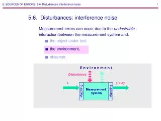
5. SOURCES OF ERRORS. 5.5. Fundamentals of low-noise design. 5.5. Fundamentals of low-noise design. 2) i dsh 2 = 2 q ( I F + I S ). I D. = 2 q ( I D + 2 I S ). 2 q I D. i df. i dsh. r d. 4) i dsh 2 = 2 q I D = 2 k T / r d. k T q I D. I D. 3) r d . r d. e dsh.

E N D
5. SOURCES OF ERRORS. 5.5. Fundamentals of low-noise design 5.5. Fundamentals of low-noise design
2) idsh2= 2q(IF+IS ) ID = 2q(ID+2IS ) 2qID idf idsh rd 4) idsh2= 2qID = 2kT/ rd kT qID ID 3) rd rd edsh Kf ID f idf rd idn2= 2qID+ , Kf= 2qff Note that dynamic resistances do not generate any thermal noise since them dissipate no power, vd id 0. 5. SOURCES OF ERRORS. 5.5. Fundamentals of low-noise design. 5.5.1. Junction-diode noise model 5.5.1. Junction-diode noise model ID VD /VT 1) ID= IS e - IS = IF-IS 5) edsh2= (2kT/ rd )rd 2 = 2kTrd At low frequencies and ID >> IS ,
vbt2= 4kTrb icsh2= 2qIC ibsh2= 2qIB Kf IB f ibf 2= 5. SOURCES OF ERRORS. 5.5. Fundamentals of low-noise design. 5.5.2. BJT noise model 5.5.2. BJT noise model C Noiseless vbt rb B icsh ibf ibsh E NB: icf =0 JC < JB,ic=hfeib,(*) ict =0 RC<0.1W, ic=hfeib *Negligible surface effects compared to FETs.
RS ic vs ? vn s RS+rb+rp hfe vn s(t)=vst(t)+vbt(t)+[ibf (t)+ibsh(t)](RS+rb) + icsh(t) 5. SOURCES OF ERRORS. 5.5. Fundamentals of low-noise design. 5.5.2. BJT noise model A. Total input noise vbt vbt rb B ip C hfe ip icsh rp ro ibf ibsh 1) Total input noise vs. time, vn s(t). 2) Power spectral density of the total input noise, vn s2(f).
? vn s vn s RS+rb+rp hfe vn s(t)=vst(t)+vbt(t)+[ibf (t)+ibsh(t)](RS+rb) + icsh(t) RS+rb+rp hfe 2 icsh2 vn s2=4kT(rb+ RS) +(ibf 2+ibsh2)(RS+rb)2+ 5. SOURCES OF ERRORS. 5.5. Fundamentals of low-noise design. 5.5.2. BJT noise model A. Total input noise RS vbt vbt rb B ip C hfe ip ic vs icsh rp ro ibf ibsh 1) Total input noise vs. time, vn s(t). 2) Power spectral density of the total input noise, vn s2(f).
vn s 2 (RS+rb)2 hfe RS+rb+hfeVT /IC hfe vn s2= 4kT(rb+ RS) +2qIC + 2qIC hfeVT (1+ hfe )0.5(RS+rb) IC opt= 5. SOURCES OF ERRORS. 5.5. Fundamentals of low-noise design. 5.5.2. BJT noise model B. Optimum collector current RS vbt rb B ip C hfe ip ic rp ro RS+rb+rp hfe 2 icsh2 vn s2=4kT(rb+ RS) +ibsh2 (RS+rb)2+ ibf =0 Reference: [7]
rb+rp hfe 2 en2= vn s2= 4kTrb+(ibf 2+ibsh2)rb2+ icsh2 RS= RS=0 icsh2 hfe2 vn s2 RS2 in2==ibf 2+ ibsh2+ 5. SOURCES OF ERRORS. 5.5. Fundamentals of low-noise design. 5.5.2. BJT noise model C. en- in noise model RS en rb B ip C hfe ip ic vs in rp ro RS+rb+rp hfe 2 icsh2 vn s2=4kT(rb+ RS) +(ibf 2+ibsh2)(RS+rb)2+
en in 5. SOURCES OF ERRORS. 5.5. Fundamentals of low-noise design. 5.5.2. BJT noise model BJT en- in noise model f >> ff rb= 100 W IC = 1 mA hfe= 100 en=1.36 nV/Hz0.5 in=1.8 pA/Hz0.5 en /in=756 W RS= 756 W in RS= 1.4 nV/Hz0.5 C B E rb+rp hfe 2 en2= 4kTrb+(ibf 2+ibsh2)rb2+ icsh2 icsh2 hfe2 in2=ibf 2+ ibsh2+
IC opt IC opt 5. SOURCES OF ERRORS. 5.5. Fundamentals of low-noise design. 5.5.2. BJT noise model D. Optimum source resistance at IC opt RS en rb B ip C hfe ip ic vs rp ro in en in = rb21+1+hfe Rs opt=
5. SOURCES OF ERRORS. 5.5. Fundamentals of low-noise design. 5.5.3. JFET noise model 5.4.3. JFET noise model D Noiseless G idf idt igsh S igsh2= 2qIG idt2= 4kT/(3/2gm) Kf ID f idf 2= NB: idsh =0
id vgs 5. SOURCES OF ERRORS. 5.5. Fundamentals of low-noise design. 5.5.3. JFET noise model Equivalent small-signal model gmvgs ig G D rgs ro igsh idf idt
id vgs vgs 5. SOURCES OF ERRORS. 5.5. Fundamentals of low-noise design. 5.5.3. JFET noise model Equivalent small-signal model gmvgs ig G D rgs ro 1/gm igsh idf idt
vgs 5. SOURCES OF ERRORS. 5.5. Fundamentals of low-noise design. 5.5.3. JFET noise model Equivalent small-signal model gmvgs ig G D ro ~1/gm igsh idf idt
RS id vs vgs ? vn s 5. SOURCES OF ERRORS. 5.5. Fundamentals of low-noise design. 5.5.3. JFET noise model A. Total input noise gmvgs ig G D ro ~1/gm igsh idf idt 1) Total input noise vs. time, vn s(t).
igsh Rs RS vs ? vn s vn s(t)=vst(t)+igsh(t)RS+[idf (t)+idt(t)](1/gm) 5. SOURCES OF ERRORS. 5.5. Fundamentals of low-noise design. 5.5.3. JFET noise model A. Total input noise gmvgs ig G D id vgs ro ~1/gm igsh idf idt 1) Total input noise vs. time, vn s(t).
RS vs ? vn s vn s vn s(t)=vst(t)+igsh(t)RS+[idf (t)+idt(t)](1/gm) 2) Power spectral density of the total input noise, vn s2(f). vn s2=4kTRS +igsh2RS2+(idf 2+idt2)/gm2 5. SOURCES OF ERRORS. 5.5. Fundamentals of low-noise design. 5.5.3. JFET noise model A. Total input noise gmvgs igsh Rs ig G D id vgs ro ~1/gm idf idt 1) Total input noise vs. time, vn s(t).
en in ? vn s vn s en2= vn s2= (idf 2+idt2)/gm2 RS = RS =0 vn s2 RS2 in2==igsh2 5. SOURCES OF ERRORS. 5.5. Fundamentals of low-noise design. 5.5.3. JFET noise model B. en- in noise model gmvgs igsh Rs RS ig G D id vs vgs ro ~1/gm idf idt vn s2=4kTRS +igsh2RS2+(idf 2+idt2)/gm2
en in 5. SOURCES OF ERRORS. 5.5. Fundamentals of low-noise design. 5.5.3. JFET noise model BJT JFET en- in noise model f >> ff Vp = 2 V IDSS= 10 mA IG = 10 pA en=1.8 nV/Hz0.5 in=1.8 fA/Hz0.5 en /in=1 MW RS= 1 MW in RS= 1.8 nV/Hz0.5 f >> ff rb= 100 W IC = 1 mA hfe= 100 en=1.36 nV/Hz0.5 in=1.8 pA/Hz0.5 en /in=756 W RS= 756 W in RS= 1.4 nV/Hz0.5 D G S en2= (idf 2+idt2)/gm2 in2=igsh2
idt2= 4kT/(3/2gm) Kf ID f idf 2= 5. SOURCES OF ERRORS. 5.5. Fundamentals of low-noise design. 5.5.4. MOSFET noise model 5.5.4. MOSFET noise model D Noiseless G idt idf S NB: igsh =0 idsh =0
RS id vs ? vn s vn s vn s(t)= vst(t)+[idf (t)+idt(t)](1/gm) vn s2=4kTRS +(idf 2+idt2)/gm2 5. SOURCES OF ERRORS. 5.5. Fundamentals of low-noise design. 5.5.4. MOSFET noise model A. Total input noise gmvgs G D ro 1/gm idf idt 1) Total input noise vs. time, vn s(t). 2) Power spectral density of the total input noise, vn s2(f).
en in en2= vn s2= (idf 2+idt2)/gm2 RS = RS =0 vn s2 Rs2 in2== 0 5. SOURCES OF ERRORS. 5.5. Fundamentals of low-noise design. 5.5.4. MOSFET noise model B. en- in noise model vn s gmvgs RS G D id vs ro 1/gm vn s2=4kTRS +(idf 2 +idt2)/gm2
5. SOURCES OF ERRORS. 5.5. Fundamentals of low-noise design. 5.5.4. MOSFET noise model JFET MOSFET en- in noise model f >> ff Vp = 2 V IDSS= 10 mA IG = 10 pA en=1.8 nV/Hz0.5 in=1.8 fA/Hz0.5 en /in=1 MW RS= 1 MW in RS= 1.8 nV/Hz0.5 f >> ff Vp = 2 V IDSS= 10 mA en=1.8 nV/Hz0.5 D en G S en2= (idf 2+idt2)/gm2 in= 0
5. SOURCES OF ERRORS. 5.5. Fundamentals of low-noise design. 5.5.5. Frequency response effect 5.5.5. Frequency response effect The aim is to analyze the dependence of a transistor en and in on frequency and the operating point. VCC iC RS vs VBB Cm vbt vbt RS rb B C hfe ip ic ip Cp vs icsh rp ro ibf ibsh
5. SOURCES OF ERRORS. 5.5. Fundamentals of low-noise design. 5.5.5. Frequency response effect A. Total input noise Cm RS rb is B C hfe ip ic ip Cp vs rp ro 1) Transconductance gain (icm<< hfe ip) ic vs hfe [1/j2pf(Cp+Cm )]/[rp+1/j2pf(Cp+Cm )] RS +rb+rpII[1/j2pf(Cp+Cm )] ___ Ag = ____________________________________ is=1 hfe /(RS +rb+rp ) 1+j2pft = _____________ , t = [(RS + rb)IIrp ](Cp+Cm )
vn s 5. SOURCES OF ERRORS. 5.5. Fundamentals of low-noise design. 5.5.5. Frequency response effect Cm vbt vbt RS rb B C hfe ip ic ip Cp vs icsh rp ro ibf ibsh hfe /(RS +rb+rp ) 1+j2pft Ag= _____________ , t = [(RS + rb)IIrp ](Cp+Cm ) 2) Power spectral density of the total input noise, vn s2(f). RS +rb+rp hfe 2 [1+(2pft)2] icsh2 vn s2=4kT(RS +rb)+(ibf 2+ibsh2)(RS+rb)2+
RS = RS =0 5. SOURCES OF ERRORS. 5.5. Fundamentals of low-noise design. 5.5.5. Frequency response effect RS +rb+rp hfe 2 [1+(2pft)2] icsh2 vn s2=4kT(RS +rb)+(ibf 2+ibsh2)(RS+rb)2+ t = [(RS + rb)IIrp ](Cp+Cm ) 3) en and in of the transistor. rb+rp hfe 2 en2= vn s2= 4kTrb+(ibf 2+ibsh2)rb2 + [1+(2pften)2] icsh2 ten= (rbIIrp )(Cp+Cm ) icsh2 hfe2 vn s2 RS2 = ibf 2+ibsh2 + [1+(2pftin)2] in2= tin= rp (Cp+Cm )
en in 5. SOURCES OF ERRORS. 5.5. Fundamentals of low-noise design. 5.5.5. Frequency response effect B. en- in noise model for high-frequencies Cm RS rb B C hfe ip ic ip Cp vs rp ro rb+rp hfe 2 en2= 4kTrb+(ibf 2+ibsh2)rb2 + [1+(2pften)2] icsh2 ten= (rbIIrp )(Cp+Cm ) icsh2 hfe2 ibf 2+ibsh2 + [1+(2pftin)2] in2= tin= rp (Cp+Cm )
5 0 4 -20 3 2 -40 1 Ag Ag max dB 100 101 102 103 104 105 106 107 108 109 ____ 100 101 102 103 104 105 106 107 108 109 f, Hz 5. SOURCES OF ERRORS. 5.5. Fundamentals of low-noise design. 5.5.5. Frequency response effect C. en(f)for differentIC rb+rp hfe 2 en2= 4kTrb+(ibf 2+ibsh2)rb2 + [1+(2pften)2] icsh2 IC opt= 24 mA IC = 0.1 mA en(f) nV/Hz0.5 rb= 100 W hfe= 100 Cm = 1 pF Cp (1 mA)= 100 pF
8 0 6 -20 4 2 -40 0 Ag Ag max dB ____ 5. SOURCES OF ERRORS. 5.5. Fundamentals of low-noise design. 5.5.5. Frequency response effect D. in(f)for differentIC icsh2 hfe2 ibf 2+ibsh2 + [1+(2pftin)2] in2= IC opt= 24 mA IC = 0.1 mA in(f) pA/Hz0.5 100 101 102 103 104 105 106 107 108 109 rb= 100 W hfe= 100 Cm = 1 pF Cp (1 mA)= 100 pF 100 101 102 103 104 105 106 107 108 109 f, Hz
V(INOISE)*1G V(Out1)/V(V1:+)/10 V(ONOISE)*1G/10 5. SOURCES OF ERRORS. 5.5. Fundamentals of low-noise design. 5.5.5. Frequency response effect E. Noise simulation inPSPICE 30 20 10 0 1.0Hz 10KHz 100MHz 1.0THz Frequency
rb= 40 W hfe= 500 ro = IC = 1 mA IDSS= 2 mA Vp= 2 V ro = ID = 1 mA RS+rb+rp hfe 2 icsh2 vn s2=4kT(rb+ RS) +(ibf 2+ibsh2)(RS+rb)2+ vn s2=4kTRS +igsh2RS2+(idf 2+idt2)/gm2 vn s2=4kTRS +(idf 2+idt2)/gm2 5. SOURCES OF ERRORS. 5.5. Fundamentals of low-noise design. 5.5.6. Comparison of the BJT, JFET and MOSFET 5.5.6. Comparison of the BJT, JFET and MOSFET
IC opt 5. SOURCES OF ERRORS. 5.5. Fundamentals of low-noise design. 5.5.6. Comparison of the BJT, JFET and MOSFET 100 Amplitude spectral density of the total input noise vn s as a function of RS vn s nV/Hz0.5 5 The 1/f noise is neglected. The JFET gate current is neglected. 1 102 103 104 105 RS, W
RS = 100 W RS = 10 kW 5. SOURCES OF ERRORS. 5.5. Fundamentals of low-noise design. 5.5.5. Frequency response effect Example: Comparison of an BJT and JFET in PSPICE en at S = 4kTRS +en 2 +2ren in +(in RS)2
5. SOURCES OF ERRORS. 5.5. Fundamentals of low-noise design. 5.5.6. Comparison of the BJT, JFET and MOSFET MOSFET Conclusion: Guide for selection of the preamplifier JFET IC amplifiers BJT Transformer coupling 1 10 100 1 k 10 k 100 k 1 M 10 M 100 M 1 G 10 G 100 G Source resistance, RS Reference: [9]
vbt rb B C hfe ip ip io icsh rp ro vst ibf ibsh E RS vct vet vs RE RC 5. SOURCES OF ERRORS. 5.5. Fundamentals of low-noise design. 5.5.7. Example circuit 5.5.7 Noise analysis of a CE amplifier VCC RC RS vs RE VBB ro
? vn s 5. SOURCES OF ERRORS. 5.5. Fundamentals of low-noise design. 5.5.7. Example circuit • Our final aim is to find and minimize the total input noise vn s. vbt rb B C hfe ip ip io icsh rp vst ibf ibsh E RS vet vct vs RE RC • Let us first find vn s by applying superposition.
io vs AOL 1+AOLb As =Gs + Gs bs fwd ___ _______ -hfe 1+hfe RE/(RE +RS+rb+rp) 1 RS+rb+rp+RE As= +0 ____________________ ___________ 5. SOURCES OF ERRORS. 5.5. Fundamentals of low-noise design. 5.5.7. Example circuit • 1) Signal gain As for vs, vst, vbt, and vet. vbt rb B C hfe ip ip io rp vst E RS vet vs RE RC
io ibf AOL 1+AOLb Abf =Gbf + Gbf bbf fwd ___ _______ RS+rb+RE RS+rb+RE +rp hfe 1+hfe RE/(RE +RS+rb+rp) Abf= +0 ____________________ ___________ 5. SOURCES OF ERRORS. 5.5. Fundamentals of low-noise design. 5.5.7. Example circuit • 2) Noise gain Abf for ibf and ibsh. rb B C hfe ip ip io rp ibf ibsh E RS vs RE RC
io icsh AOL 1+AOLb Acsh =Gcsh + Gcsh bcsh fwd ___ _______ hfe 1+hfe RE/(RE +RS+rb+rp) RE RE +RS+rb+rp Acsh= -1 ____________________ - ___________ 5. SOURCES OF ERRORS. 5.5. Fundamentals of low-noise design. 5.5.7. Example circuit • 3) Noise gain Acsh for icsh. rb B C hfe ip ip io icsh rp E RS vs RE RC
io vct Act =Dct ___ 1 RC Act= - ___ 5. SOURCES OF ERRORS. 5.5. Fundamentals of low-noise design. 5.5.7. Example circuit • 4) Noise gain Act for vct. rb B C hfe ip ip rp E RS io vs vct /RC RE RC
vn s (ibf +ibsh)Abf As icsh Acsh As vct Act As vn s(t) = vst +vbt +vet + + + __________ _______ _____ (RSbE+rp)2 hfe2 1 RC As2 +icsh2 + 4kT ________ _____ vn s2(f) = 4kTRSbE+(ibf 2+ibsh2)RSbE2 0 5. SOURCES OF ERRORS. 5.5. Fundamentals of low-noise design. 5.5.7. Example circuit • 5) Total input noise vs. time, vn s. rb B C hfe ip ip io icsh rp RS ibf ibsh E vs RE RC RSbE =RS +rb+RE
rb en in E RE (RbE+rp)2 hfe2 en2 =en s2 =4kTRbE+(ibf 2+ibsh2) RbE2+ icsh2 RS = RS =0 5. SOURCES OF ERRORS. 5.5. Fundamentals of low-noise design. 5.5.7. Example circuit 6) en- in noise model. B C hfe ip ic ip rp RC E RS vs (1+hfe)RE RbE= rb +RE en s2 RS2 icsh2 hfe2 in2 ==ibf 2+ibsh2+
0 1.4 1.2 -0.1 en s norm. dB en s norm. dB 1.0 hfe=104 -0.2 0.8 hfe=103 0.6 hfe=102 -0.3 0.4 -0.4 0.2 0 -0.5 102 103 104 0.1 1 10 IC /IC opt hfe hfeVT (1+ hfe )0.5RSbE IC opt= (1+hfe )0.5 (1+hfe )0.5-1 vn s min2=4kTRSbE 5. SOURCES OF ERRORS. 5.5. Fundamentals of low-noise design. 5.5.7. Example circuit 7) Minimizing CE noise. rb= 100 RS= 200 RE= 200 ibf 2= 0 vbt2= 4kTrb vet2= 4kTRE ibsh2= 2qIC /bicsh2= 2qIC 2 RSbE2 hfe RSbE+hfeVT /IC hfe vn s2= 4kTRSbE+ 2qIC +2qIC Reference: [7]
Next lecture Next lecture: