Download
1 / 15
150 likes | 314 Views
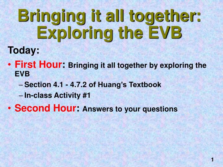
Bringing it all together: Exploring the EVB. Today: First Hour : Bringing it all together by exploring the EVB Section 4.1 - 4.7.2 of Huang’s Textbook In-class Activity #1 Second Hour : Answers to your questions. Recap: M6811 Datapath. Internal Bus #1. Register File (A, B, IX, IY, IR).

E N D
Bringing it all together:Exploring the EVB • Today: • First Hour: Bringing it all together by exploring the EVB • Section 4.1 - 4.7.2 of Huang’s Textbook • In-class Activity #1 • Second Hour: Answers to your questions
Recap: M6811 Datapath Internal Bus #1 Register File (A, B, IX, IY, IR) Memory Address M M CCR Data Bus Bus P ALU A B C R R A16- A0 D7- D0 MUX Internal Bus #2 The datapath unit consists of registers, buses connecting them, and the ALU
Control Unit Recap: M6811 Control Unit Internal Bus #1 Register File (A, B, IX, IY, IR) Memory Address M M CCR Data Bus Bus P ALU A B C R R A16- A0 D7- D0 MUX Internal Bus #2
Recap: Time-Multiplexed Bus 1 MODB 1 MODA E R/W AS 68HC11 A15 - A8 PB7- PB0 Bus AD7 - AD0 PC7- PC0 Other pins not shown
Recap: Bus Timing Diagram XTAL Magic Moment #2 E R/W A15-A8 HI ADDR AD7-AD0 LO-ADDR DATA AS Magic Moment #1
Recap: De-multiplexing the Address 1 MODB 1 MODA E R/W AS 68HC11 Address A0-A7 latched on the falling edge of AS A15-A8 PB7-PB0 Bus AD7-AD0 PC7-PC0 Magic Moment #1 Other pins not shown D0-D7 LE 0 OE LS 373 Q0-Q7 A0-A7
Step 1: Bus Demultiplexing Use address strobe (AS) and a latch to Demultiplex the address and data lines Step 2: Address Decoding Use Boolean logic to decode the desired address Chip Select = Compare(A15… A0 = desired address ) AND (E = 1) Step 3: Generate Read/write control signal Use the second half of E cycle to generate Read/Write signal for RAM chip Bus Interfacing Summary
Recap: Memory Interfacing Decoder A15 A2 $4000 - $5FFF A14 A1 O2 A13 A0 E E3 V E2 E1 DD 68HC11 CS2 CS1 74LS00 WE R/W 74LS04 A12 – A8 A12-A0 Latch AS LE 8K RAM O7-O0 AD7-AD0 D7-D0 OE OE I/O8 - I/O1
Every I/O device “appears” to the CPU as a memory location Use LDAA and STAA for input/output Several useful I/O devices, and some memory devices are already interfaced for us on the 6811 chip. Recap: Memory-mapped I/O
Event counter Periodically check the chip PA7 PAI ROM-8KB PULSE ACCUMULATOR OC2 O PA6 C OC3 PA5 1 PORT PA4 OC4 RAM-256 bytes OC5 A PA3 IC1 PA2 PERIODIC INTERRUPT PA1 IC2 EEPROM-512 bytes COP WATCHDOG IC3 PA0 PE7 PD5 SS SCK PD4 PE6 SPI PE5 MOSI PD3 PORT PE4 PD2 MISO PORT DATA DIRECTION A/D E PE3 D CONVERTER PE2 PD1 TxD SCI PE1 RxD PD0 PE0 V REFH M68HC11 CPU V REFL ADDRESS DATA BUS RESET INTERRUPTS XIRQ IRQ HANDSHAKE I/O (V ) PPBULK DATA DIRECTION C XTAL PARALLEL I/O OSCILLATOR PORT B PORT C EXTAL E P P P P P P P P P P P P P P P P S S SINGLE MODA B B B B B B B B C C C C C C C C T T MODE CHIP LIR 7 6 5 4 3 2 1 0 7 6 5 4 3 2 1 0 R R SELECT MODB B A (V ) STBY A A A A A A A A A A A A A A A A AS 1 1 1 1 1 9 8 D D D D D D D D R/W 1 V EXPAND DD 5 3 2 1 0 7 6 5 4 3 2 1 0 4 POWER V SS Put code in ROM Fancy general-purpose timer Put non-volatile data in EEPROM Generate periodic interrupts SPI for inter-connecting 6811’s Input analog signals SCI for connecting to host computer Bus for expansion
Recovers PORTB and PORTC in expanded mode Port Replacement Unit (PRU) 1 MODB 1 MODA E R/W AS PORTB 68HC11 Port Replacement Unit (PRU) PORTC A15-A8 PB7-PB0 STRA AD7-AD0 PC7-PC0 STRB Other pins not shown
Building The EVB Port A AD0 - AD7 PD0 - 5 6811 A0 - A7 Latch Port E A0 – A15 A8 – A15 8K RAM 8K ROM Port B PRU Port C AD0 - AD7
Adding Communication Host Computer (P3) PD1 Port A RX TX PD0 AD0 - AD7 PD0 - 5 6811 Control A0 - A7 Latch Port E A0 – A15 A8 – A15 RS-232 Drivers & Receivers 8K RAM 8K ROM Terminal (P2) ACIA Port B TX TX PRU Port C RX RX AD0 - AD7 Control
Memory Map Specifies what addresses are for what BUFFALO Utility Routines Useful for development & debugging BUFFALOcommand interpreter Interrupt vector jump table in RAM Software Picture of EVB
Do Activity #1 Now • Due: End of Class Today. • RETAIN THE LAST PAGE(S) (#3 onwards)!! • During studio time this week: • Catch up with experiments. • Summarize reading of Chapter 4, Chapter 5 (sections 5.1-5.4), and Chapter 6 (6.1 – 6.7) That’s it. No more new material!