Download
1 / 24
240 likes | 428 Views
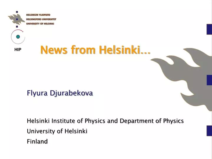
Flyura Djurabekova. News from Helsinki…. Helsinki Institute of Physics and Department of Physics University of Helsinki Finland. Outline. Basic outline of activities at Helsinki Institute of Physics and not only Multiscale/ multiphysics model to describe an arcing event News:

E N D
Flyura Djurabekova News from Helsinki… Helsinki Institute of Physics and Department of Physics University of Helsinki Finland
Outline • Basic outline of activities at Helsinki Institute of Physics and not only • Multiscale/multiphysics model to describe an arcing event • News: • Novel view on the “worm”-like features found in high resolution SEM images of electrical breakdown spots • The latest simulations coupling the dislocation activity in a stress concentrator and effect of electric field
Problem at hand Setup to measure dc sparks on a flat cathode surface (CERN)
Problem at hand Means for solution: a Model?
…Multiscale/multiphysics computational model to simulate electrical breakdown Stage 1:Charge distribution @ surface Method:DFT with external electric field ~few fs Stage 2: Atomic motion & evaporation + Joule heating (electron dynamics) Method: Hybrid ED&MD model (includes Laplace and heat equation solutions) ~fewns ~ sec/min ~ sec/hours Stage 3a: Onset of tip growth; Dislocation mechanism Method:MD, ED+MD, FEM… Stage 3b:Evolution of surface morphology due to the given charge distribution Method:Kinetic Monte Carlo R. Behrisch, Plenum, 1986 B. Jüttner, 1979 Stage 4:Plasma evolution, burning of arc Method:Particle-in-Cell (PIC) ~10s ns ~100s ns Stage 5: Surface damage due to the intense ion bombardment from plasma Method:Arc MD
University of Helsinki, Finland Behind the model… Doc. Flyura Djurabekova Senior scientist Prof. Kai Nordlund M Sc AarnePohjonen Dislocations M Sc Stefan Parviainen Field emisssion and neutral atom evaporation M Sc AvazRuzibaevCharges on surfaces Dr LottaMether Plasma simulations CERN, Switzerland M Sc Anders KorsbäckExperiments at CERN Dr. Yinon Ashkenazy Hebrew University Israel Dr. VahurZadin University of Tartu Estonia Inspiration from and constant discussions with CERN, Geneva … and many other colleagues from CLIC project, KEK and SLAC Dr. Walter Wuensch Sergio Calatroni
High resolution SEM: new features called ”flowers” or ”spaghetti” • The halos seen around the breakdown spots were well identified in HR-SEM as the dense network of white lines (in SEM images) of uncertain origin SEM images here after are courtesy to presentation by Markus Aicheler at “MeVArc-2012”
Fine ”flowers” as plastic response of surface on a sparking strike • The “flowers” spread well beyond the actual breakdown spots
Vectorized image • Binarize “flowers” to be analyzed by a computer r
Filtered view • Filter out the undistinguishable areas to reduce the unnecessary noise in the analysis
Fit in polygons • Polygons are fit in the white areas, which of course is not always perfect, but sufficiently close
Angle distribution gives a peak at 60o • Peak at 60 degree indicates a dislocation origin of the white ”worms” features. The most straightforward thought is that the slip planes intersect each other on Cu {111}-surface at 60o.
Experimental evidence that there is some correlation between the “worms” and grains with 111 oriented surfaces • All the experimental analysis of surface structure is courtesy of Markus Aicheler IPF coloring EBSD data All Euler coloring EBSD data
Wormsagainst the randomwalkers • We have also ran some 2D random walk simulations , but did not find the regular patterns seen in the “worms”
Electrodynamics-molecular dynamic model+ study of a void under tensile stress • ED-MD model follows the evolution of the charged surface. • The dynamics of atom charges follows the shape of electric field distortion on tips on the surface • Wealsostudies the dislocationdynamics on a voidburrowednear the surface in Cuheldunderunilatertensilestress. Details in F. Djurabekova, S. Parviainen, A. Pohjonen and K. Nordlund, PRE 83, 026704 (2011). A. Pohjonen, F. Djurabekova, et al., Jour. Appl. Phys. 110, 023509 (2011).
Back to simulation with assumed voids under surface • We have now finished the analysis of the behavior of a void under tensile stress due to the electric field (Simulations now done with the hybrid ED-MD code, where the electric field effect is accounted explicitly)
The gradual growth seen previously is “catastrophic” in the presence of the field • The analysis of the protrusion height increase shows an asymptotic character. Once it starts growing, the self-reinforcing effect of the field enhancement around the tip of the protrusion causes the increase of its height in the ”catastrophic” manner
Initial plastic deformation • the top view and a slice of the system at time t = 114 ps when the first bump has formed
“Catastrophic”growth of a protrusion at the void • . the top view and a slice of the system at time t = 130 ps when the fully developed protrusion is clearly visible.
Analysis of the shear stress near the void surface • We analyzed more carefully the stresses at the void surface • We find that even if the void is burrowed in the bulk the shear stress is more than half of the value of tensile stress at the surface
Deeperview on atomiclevelstress • The distribution of shear stress xz on MD simulations along a line (directed in z-direction) starting from the point of maximum shear on void surface and ending on the material surface for a void located at depth H = 2R. b) A detailed view of the atomic level stress near the void surface shows an alternating pattern caused by the surface stress. c) The difference between the simulation results with external stress and pure surface stress corresponds to the analytical result.
Summary • The model has been actively developed and gave many new insights in the physics of the plasma onset and surface damage • The model underlines the importance of mechanical properties of metal surfaces • We also noticed these to be important for surface damage • Angular analysis showed a dislocation origin of “worm”-like features around breakdown spots • The coupling of dislocation model and electric field effect resulted in “catastrophic” protrusion growth, which was not observed previously, but intuitively in line with field emission measurements from flat copper surfaces.
Thankyou for attention and valuable feedback! Accelerator Laborary, Helsinki