Slide Note
0 likes | 1 Views
A combinational circuit consists of logic gates that produce outputs based on current inputs, following Boolean functions. These circuits transform binary information from inputs to outputs through interconnections of gates. Analysis involves verifying circuit type, deriving Boolean functions, and creating truth tables. The design process includes defining objectives, creating truth tables, simplifying Boolean functions, and verifying designs with logic diagrams. Binary adder-subtractor circuits are fundamental for arithmetic operations in digital computers, built hierarchically from half adders to full adders.

E N D
Combinational Logic Chapter 4 Digital Logic Design-5ed
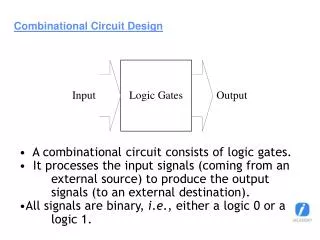
Combinational Logic: Definition • A combinational circuit consists of logic gates whose outputs at any time are determined from only the present combination of inputs. • A combinational circuit performs an operation that can be specified logically by a set of Boolean functions.
Combinational Logic: explanation • A combinational circuit consists of an interconnection of logic gates. Combinational logic gates react to the values of the signals at their inputs and produce the value of the output signal, transforming binary information from the given input data to a required output data.
Combinational Logic: explanation • The n input binary variables come from an external source; the m output variables are produced by the internal combinational logic circuit and go to an external destination. • Each input and output variable exists physically as an analog signal whose values are interpreted to be a binary signal that represents logic 1 and logic 0. • For n input variables, there are 2n possible combinations of the binary inputs. • For each possible input combination, there is one possible value for each output variable.
Combinational Logic: explanation • A combinational circuit can be specified with a truth table that lists the output values for each combination of input variables. • A truth table for a combinational circuit consists of input columns and output columns. The input columns are obtained from the 2n binary numbers for the n input variables. The binary values for the outputs are determined from the stated specifications. The output functions specified in the truth table give the exact definition of the combinational circuit. • A combinational circuit also can be described by m Boolean functions, one for each output variable. • Each output function is expressed in terms of the n input variables.
Analysis of combinational Logic • Verify that the circuit diagram is combinational • Obtain the output Boolean functions or the truth table • To obtain the output Boolean functions from a logic diagram, we proceed as follows: • 1. Label all gate outputs that are a function of input variables with arbitrary symbols, but with meaningful names. Determine the Boolean functions for each gate output. • 2. Label the gates that are a function of input variables and previously labeled gates with other arbitrary symbols. Find the Boolean functions for these gates. • 3. Repeat the process outlined in step 2 until the outputs of the circuit are obtained. • 4. By repeated substitution of previously defined functions, obtain the output Boolean functions in terms of input variables.
Analysis of combinational Logic • Obtain the truth table directly from the logic diagram without going through the derivations of the Boolean functions, we proceed as follows: • 1. Determine the number of input variables in the circuit. For n inputs, form the 2n possible input combinations and list the binary numbers from 0 to (2n - 1) in a table. • 2. Label the outputs of selected gates with arbitrary symbols. • 3. Obtain the truth table for the outputs of those gates which are a function of the input variables only. • 4. Proceed to obtain the truth table for the outputs of those gates which are a function of previously defined values until the columns for all outputs are determined.
DESIGN PROCEDURE DESIGN PROCEDURE The design of combinational circuits starts from the specification of the design objective and culminates in a logic circuit diagram or a set of Boolean functions from which the logic diagram can be obtained. The procedure involves the following steps: • 1. From the specifications of the circuit, determine the required number of inputs and outputs and assign a symbol to each. • 2. Derive the truth table that defines the required relationship between inputs and outputs. • 3. Obtain the simplified Boolean functions for each output as a function of the input variables. • 4. Draw the logic diagram and verify the correctness of the design (manually or by simulation).
BINARY ADDER BINARY ADDER– –SUBTRACTOR SUBTRACTOR • Digital computers perform a variety of information-processing tasks. Among the functions encountered are the various arithmetic operations. The most basic arithmetic operation is the addition of two binary digits. This simple addition consists of four possible elementary operations: 0 + 0 = 0 0 + 1 = 1 1 + 0 = 1 1 + 1 = 10.
BINARY ADDER BINARY ADDER– –SUBTRACTOR SUBTRACTOR • Definition: • A binary adder–subtractor is a combinational circuit that performs the arithmetic operations of addition and subtraction with binary numbers. • The circuit is developed by means of a hierarchical design. The half adder design is carried out first, from which we develop the full adder.
Half adders • A combinational circuit that performs the addition of two bits is called a half adder . • One that performs the addition of three bits (two significant bits and a previous carry) is a full adder . • The names of the circuits stem from the fact that two half adders can be employed to implement a full adder.
Half adders • This circuit needs two binary inputs and two binary outputs. The input variables designate the augend and addend bits; the output variables produce the sum and carry. • The symbols x and y denotes the two inputs • S (for sum) and C (for carry) to the outputs. • The truth table for the half adder is listed. • The C and S are obtained by adding x and y. • The C output is 1 only when both inputs are 1. • The S output represents the least significant bit of the sum.
Half adders function • The simplified Boolean functions for the two outputs can be obtained directly from the truth table. • The simplified sum-of-products expressions are • S = x’y + xy’ • C = xy • Check out the values of S column that at how many places it has 1, note down the corresponding input x and y (if x=1 then write as x and if x=0 then write as x’) • Similarly check the next column of C for its 1’s and note down the corresponding values of inputs.
Half adders logic diagram • The logic diagram of the half adder implemented in sum of products w.r.t. to its equations • S = x’y + xy’ • C = xy
Half adders logic diagram • The logic diagram of the half adder implemented in sum of products can be simplified to • S = x’y + xy’ • C = xy • As • S = x ⊕ y • C = xy
Half Half Subtractor Subtractor: : • A half subtractor is an arithmetic circuit that subtracts two bits and produces their difference. • It performs the operation X – Y. It should be noted that the weight of the output borrow bit is -2, while the weight of the output difference bit is +1.
Half Half Subtractor Subtractor: : • The block diagram of half subtractor is shown. The circuit has two inputs minuend (X) and subtrahend (Y) and two output bits, one is the difference bit (D) and the other is the borrow bit (B). • It performs the operation X – Y. It should be noted that the weight of the output borrow bit is -2, while the weight of the output difference bit is +1. X Y B D 0 0 0 0 0 1 1 1 1 0 0 1 1 1 0 0
Half Half Subtractor Subtractor: : • The Boolean functions for the two outputs can be obtained directly from the truth table as: • D = X’Y+ XY’ • D = X ⊕ Y Logic circuit diagram of Half subtractor • B= X’Y