Download
1 / 9
90 likes | 93 Views
L2ßeta is a hardware solution that replaces DMA P/IO buffers with FPGA FIFO, providing maximum use of manufactured components and compatibility with present systems. It offers a short development time, support for L2 flushing, and a clear upgrade path to modern CPUs.

E N D
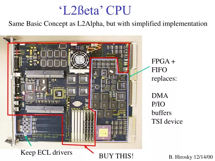
FPGA + FIFO replaces: DMA P/IO buffers TSI device Keep ECL drivers BUY THIS! ‘L2ßeta’ CPU Same Basic Concept as L2Alpha, but with simplified implementation
‘L2ßeta’ Implementation • Hardware Components • 6U VME SBC w/ integrated UII • 9U adapter card w/ custom i/o devices • PCI (PMC) to adapter bridge card Draft technical note at: www-d0.fnal.gov/~hirosky/l2b
Practical goals • Minimal engineering • Maximum use of manufactured components • (hardware/firmware) • Hardware compatibility w/ present system • MBus/VME compliance • Software (source code) compatibility w/ present system • Device driver APIs • Short development time • Support/flush out L2 if hardware set not complete • Long term solution to L2 support • freedom from parts obsolescence for repair/spares • clear upgrade path to modern/powerful CPUs
Hardware Engineering Components Interface Card: sits on PMC needs to support PCI interface on front end and local interface on back end (preferably supports 33 and 66MHz buses) Adapter Card: contains FIFO’s ECL and Mbus drivers, and control FPGA
Software/Firmware Engineering Components SBC: Linux interrupt handler Linux memory mapper Device driver code Interface Card: PCI interface module, local interface firmware Adapter Card: FPGA Firmware, controls MBus i/o, DMA
Source code compatibility - needs new PCI base classes (PCIDEV, PCICFG, CIA) the UII driver should be transparent - need new drivers for replace MB devices and TSI - easy - “minor” linux tweeks --->> result = source code compatible boards! Can select hotter CPU boards for Global worker or cooler boards for Administrators
Many vendors for SBC cards, most VME SBCs have UIIB’s on board. Small companies w/ off the shelf boards + custom options Medium companies like SBS w/ off the shelf boards Giant companies like Raytheon too! Medium and High End CPU’s available now vs. our alpha: SPECint95 SPECfp95 SBC PCI Cost Alpha 500 MHz 15.4 21.1 64/33 ~$5K (complete) PIII 800MHZ 38.4 28.4 32/33 ~$4K (SBS) (PIII 1GHz now available) POWERPC 750 22.4 13.3 32/33 (550MHz) 7400 21.4 20.4 32/33 SPARC II 18 22 64/33 ~$3.5K (Momentum) SPARC III 35+ 60+ ? N/A (Faster SPARCIIs expected)
Issues Can we live w/ a 33MHz 32-bit bus? ~(125MB/s) Probably, if we can do full speed to RAM. This is about the same as we have now! If so, could we easily upgrade to a 66MHz 32bit bus? (depends on PCI interface hardware – ie YES if ALTERA megacore or similar) Can we instead use AGP for broadcast? (>500MB/s) (Commercial prototype cards are available) Compilers for SPARC under Linux? “Experimental g++”, Linux->SPARC cross compiler,... (SOLARIS out of the question? Compilers available=KAI, SUN) Alas, KAI supports INTEL/ALPHA Linux, not SPARC Linux Linux kernal mods - expect easier time in Pentium..