Download
1 / 7
70 likes | 74 Views
It is good to know about the prototyping process when you own a business that deals with PCB products. It helps to enhance your business. You gain more expertise about it. The article explains the steps in a detailed way. Continue reading to expand your knowledge on this matter.<br><br>View more: https://www.greatpcb.com/pcb-assembly/

E N D
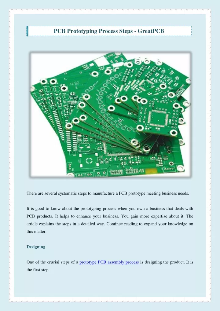
PCB Prototyping Process Steps - GreatPCB There are several systematic steps to manufacture a PCB prototype meeting business needs. It is good to know about the prototyping process when you own a business that deals with PCB products. It helps to enhance your business. You gain more expertise about it. The article explains the steps in a detailed way. Continue reading to expand your knowledge on this matter. Designing One of the crucial steps of a prototype PCB assembly process is designing the product. It is the first step.
Making a schematic design The next thing is to focus on the elements of a schematic design of the prototype PCB assembly. You gather information about the components that are parts of the production. Some simulations validate the design. Creating a BOM (Bill of Materials) The BOM or the Bill of Materials includes detailed information about every component of the PCB product. For example, the BOM tells about the number of components, reference designators, footprint, and other such things. Doing the routing design The next step is performing the routing design, which considers the aspects of power levels, generation of signal noise, its sensitivity, etc.
Checks There are vital checks in the following step that you must never overlook. You have to be sure about different functionality issues. The checks make it possible to locate the problems. Mend when you find them. Manufacturing the Photo Film The design is the foundation based on which you create the essential photo film of the PCB product. It is fundamentally a plastic sheet. The film has a photo negative. The primary material in most cases is conductive copper. Inner layer printing The following step involves printing the distinct inner layers. There is an application of UV light. It is a highly technical step. You have to strategically reveal the copper by removing the hardened and ‘not hardened photo-resist.
Aligning the multiple layers In the next step, it is a priority to align the numerous layers. It would be best if you accurately punched the registration holes. Fusing all the layers After that, you have to fuse all the layers efficiently. It will make the structure robust. A bonding press advanced computer plays an important role in this procedure. Drilling holes
The next step is all about drilling perfect holes. The diameters of the holes are in microns. You use sophisticated tools in performing the task. Copper plating You use the method of a chemical bath to execute the procedure of copper plating. In this case, too, a computer controls everything. Imaging of the outer layer In the following step, you have to process the imaging of the outer layer to add value to the product. Another round of copper plating It is essential to undertake the process of another round of copper plating to strengthen the functionality of the product. Final etching When the previous steps are complete, you can go for the procedure of final etching to give some finishing touches. Application of the solder mask and surface finish The next step involves the technical process of applying a solid solder mark and giving touches to the surface finish. Applying the silkscreen After that, you need to apply the silkscreen to strengthen the surface of the PCB product in the desired way.
Cutting There are two broad methods of cutting the PCB board. It can be via the procedure of a rooter. On the other hand, it can be a v-groove. Sourcing and Assembly After the steps mentioned above, you need to source and assemble the PCB boards in an organized way. Hire a top-rated service provider It is wise to hire a reputed and reliable service provider with many years of experience and expertise in PCB assembly.
CONTACT US CONTACT US Address: 22, Science Park, The Northern part of HeYi Village, ShaJing Town, Bao An, Shenzhen, GuangDong, China, 518104 Phone: +86-755-27810810 Fax: +86-755-27810813 Email: sales@greatpcb.com WhatsApp: +86-13682523810 Skype: GREATPCB Website: http://www.greatpcb.com