Download
1 / 23
230 likes | 260 Views
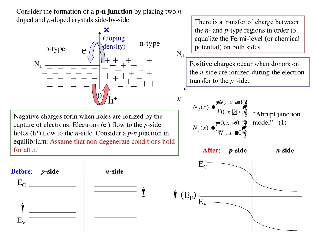
Consider the formation of a p-n junction by placing two n -doped and p -doped crystals side-by-side:. There is a transfer of charge between the n - and p -type regions in order to equalize the Fermi-level (or chemical potential) on both sides. (doping density). n-type. p-type. e -.

E N D
Consider the formation of a p-n junction by placing two n-doped and p-doped crystals side-by-side: There is a transfer of charge between the n- and p-type regions in order to equalize the Fermi-level (or chemical potential) on both sides. (doping density) n-type p-type e- Nd Na Positive charges occur when donors on the n-side are ionized during the electron transfer to the p-side. 0 h+ x “Abrupt junction model” (1) Negative charges form when holes are ionized by the capture of electrons. Electrons (e-) flow to the p-side holes (h+) flow to the n-side. Consider a p-n junction in equilibrium: Assume that non-degenerate conditions hold for all x. After: p-siden-side EC EV Before: p-siden-side EC EV (EF)
In order to describe the spatial variation in the band edges, EC and EV, we introduce a potential function, (x), such that each level is shifted by -e(x). That is, EC EC - e(x) and EV EV - e(x). Therefore, the carrier concentrations can be expressed by (2) Consider limits at x =
We can solve for the difference of the two potentials at The electric field is related to the potential by Gauss’s Law: for our 1D problem. We assume that donor and acceptor impurities are fully ionized at all x. (3) We can substitute Eqs. (1) and (2) into Eq.(3) to get a difficult nonlinear differential equation.
We can make some important approximations to simplify and solve: Assume that the potential change occurs in a finite region near the junction that is defined by -dp x dn. This is referred to as the depletion region. Also n << Nd and p << Na in this region since is closer to the middle of the gap (i.e., midgap). We can solve this problem assuming an abrupt junction model which will give a simple linear second order ordinary differential equation: Note that we have first used the boundary conditions at the edges of the depletion region (see graph on next slide) to solve for (x): The electric field must be zero outside the depletion region for equilibrium to hold. The potential must be its limiting value at the boundaries of the depletion region.
Graphical illustration of the Abrupt-junction model. p-type n-type Nd Carrier density nc(x) Na pv(x) -dp 0 dn x Depletion layer eNd Charge density (x) -dp dn x -eNa () (x) -dp dn x (-)
Comparison of the potential and electric field in the abrupt-junction model: () (x) -dp dn x (-) x There are important relations that we get by imposing continuity of (x) and ’(x). Continuity of the derivative gives:
Secondly, continuity of (x) gives Together with the derivative condition: Nddn=Nadp this gives For Na,d ranging from 1014 to 1018 cm-3 dn,p ranges from 104 to 102Å The total depletion width is LD = dn +dp We can also write this in a numerically convenient form: The maximum electric f ield within the depletion layer is of the order of / (dn+adp) and ranges from 105 to 107 volts/m.
Consider the effect of an applied voltage on the depletion width of a p-n junction: p n Charge density, (x) (x) o V = 0 “zero-bias” -dp dn x -eNa The potential simply changes according to =o|V| - sign: “Forward bias” + sign: “Reverse bias” p n p n 1(x) o- |V1| V1 > 0 “Forward-Bias” -dp dn x -eNa 2(x) We are changing the size of the depletion region by applying an external voltage. o + |V2| p n -dp dn x -eNa V2 < 0 “Reverse-Bias”
The formula for the depletion width can easily be modified to include the effects of a voltage bias: Zero-bias depletion length Consider rectification by a p-n junction. The symbol J is used for # of carriers /(area·time). The lower case symbol j is more commonly used for current density and has units j = coulombs/ (area·time). Note j e= -e J e and j h= e J h . Consider electron and hole generation currents. These carriers are generated by thermal excitation as we saw before according to p-siden-side EC EV e- (EF) Note: The generation currents involve minority carriers. h+
In a band diagram, electrons fall down hill and holes “float” uphill (both towards lowest energy). In the process of the generation currents, holes (from n-side) p-side, electrons (from p-side) n-side. Secondly, consider another kind of current, Recombination current. With this kind of current holes (from p-side) n-side. Electrons from the n-side p-side. This current involves majority carriers, and it is made possible by thermal excitation over the barrier, as shown below: Consider the hole recombination current. The current is approximated well by assuming thermionic emission over the barrier: p-siden-side EC EV o- |V1| e- (EF) h+ The middle equation is a statement that no net current can flow during equilibrium when V=0.
The total hole current from the p to the n-side is given by the recombination current minus the generation current: Note: In our notation Jh and Jp will mean the same thing. p n The last equation includes the currents of both holes and electrons, since the same analysis will also apply to electrons. It is obvious to understand the rectifying properties of a p-n junction (diode) from this equation. V Reverse bias (V<0) Forward bias (V>0) j Rectifying behavior of a p-n junction (diode). V Saturation We still need to calculate this term in terms of fundamental parameters describing transport.
In a more general treatment, it is not necessary to separate into generation and recombination currents. Note that to solve for the following five fundamental quantities (Je(x), Jh(x), n(x), p(x), and (x)), we need five equations. In the equilibrium case with V=0, Je(x)= Jh(x)=0, we need three equations to solve the three unknowns, including Poisson’s equation for the potential. In the presence of a field E and n and p, we can write the electron and hole current densities as: Where n and p are the electron and hole mobilities in units of cm2/V·s, and Dn and Dp are the electron and hole diffusion constants in units of cm2/s When dn/dx=0, From the Dude theory (mv=Ft) recall Therefore, Which expresses in terms of the collision time and masses, based on the Drude model.
Now, recall that At equilibrium, These last two relations are known as the Einstein relations. Consider continuity equations for transport of charge: If V0 and carriers are conserved. We have to include two other processes which act as a source and drain for carriers: (i) Generation by thermal excitation (ii) Recombination (electron hole) EC EV (i) (ii) As a result the continuity equations need to include these additional terms:
The g-r terms act to restore the system to equilibrium when the system deviates from equilibrium. These terms can be further described by electron and hole lifetimes (n and p): where no and po are equilibrium concentrations as determined by the law of mass action. Note that n >>ncol and p >>pcol ; typically n ~10-9 s and ncol ~10-13 s p n Very often we deal with a steady state condition in which This gives V For V0, we are not in equilibrium but we have a steady state for V = const. Note that Je = Jh = 0 for V = 0 n = no and p = po. Now suppose that E0, i.e., the electric field is negligible. Then Fick’s Law for Diffusion
Therefore, further give the following 2nd order ordinary differential equations which are referred to as diffusion equations: Note no and po are equilibrium values. The solutions are easily written as: The diffusion lengths Lp and Ln are given by Note that when E0, the majority carrier density is constant and the carriers in the diffusion equation are for the minority carriers. For example if we have a p-type material pn = ni2 and p >> n so that electrons (np) are minority carriers. The notation is slightly changed to be more precise: p-type n-type
Examine the meaning of the diffusion lengths, Ln and Lp. Since From the equipartion theorem and Drude approximation: ½ mvth2 = 3/2 kBT Further, the mean free path lnis given by ln=vthcol where vthis the thermal velocity of a carrier. The interpretation here is as follows: When a carrier undergoes N collisions before recombination, the net displacement will be The factor of 3 comes from the number of degrees of freedom (3D). This is basically a “random walk” problem. 4 Note that n >>ncol and p >>pcol ; typically n ~10-9 s and ncol ~10-13 s N3000 as the number of collisions before recombination in GaAs. 2 1 3
We need to improve our understanding of transport across the p-n junction. Consider an equivalent description of Boltzmann statistics at thermal equilibrium: whereni is the intrinsic carrier concentration EF = is the Fermi-level (or chemical potential), and Eiis the position of the chemical potential for the intrinsic case. Remember that Let us define potentials = -Ei/e and = -EF/e. At thermal equilibrium pn=ni2 (V=0 across the junction). For the case of V0, we can write the carrier concentrations as Where n and p are called quasi-Fermi levels or imrefs(imaginary references). The advantage of this formalism is that the potential difference V across the junction is just the difference in the quasi-Fermi levels, i.e.
Forward-Bias Conditions Reverse-Bias Conditions p-side n-side p-side n-side E (eV) E (eV) EC -ep -en EF () EC -ep -en EF () EV EV -dp 0 dn x -dp 0 dn x Potential Potential p n V -V n p Note that (dp+dn) for reverse bias is greater than (dp+dn) for forward bias. -dp 0 dn x -dp 0 dn x ppo log(n,p) ppo log(n,p) nno nno ni ni pn np pno npo pno npo pn -dp 0 dn x np -dp 0 dn x
For a forward bias V = p-n > 0 and pn > ni2 in the junction. The opposite is the case for a reverse bias V = p-n < 0 and pn < ni2 . Now consider the current density and write in terms of and : Our previous notation was Note that In the depletion layer –dp < x <dp Similarly, For p and n constant, Je and Jp are 0. since n and p are sharply decreasing functions in the depletion layer. Also, we assume that passage of carriers across the junction is very fast so that generation and recombination currents in the depletion region are negligible. This leads to assumption that Je and Jp are constant in the depletion region –dp < x <dp
Consider n at x = -dp (on the p-side): (1) Note that npo is the electron density on the p-side at x = -. Similarly, at x = +dn And pno is the hole density on the n-side at x = + (2) These equations serve as boundary conditions for the I-V equation of the ideal p-n junction. Recall that just outside of the depletion region (i.e. |x| > dn, dp the region is neutral, E0, and this is called the diffusion region. In these regions, the following diffusion equations apply for the respective minority carrier densities: Using boundary conditions (1) and (2), the solutions are: Note that the expected limits are observed: np npo at x = - while pn pno at x = +
We can now calculate the electron and hole currents entering the diffusion region where E0. At x = dn for the n-side. for the p-side. The total current is given by J = Je + Jp where This result is the well known Shockley equation. Previously we wrote the current in terms of electron and hole generation currents: Note that (on p-side) and (on n-side) Contains fundamental parameters describing the rectifying behavior.
Examine the minority carrier densities and current densities for forward and reverse bias: p-side n-side p-side n-side n,p n,p pn np pno pno npo npo np pn -dp 0 dn x -dp 0 dn x J=Jn+Jp J J Jp J=Jn+Jp Jn Jp Jn -dp 0 dn x -dp 0 dn x Note that (dp+dn) for reverse bias is greater than (dp+dn) for forward bias. Forward Bias (V >0) Reverse Bias (V<0)
Possible to examine details of diffusion, using the Haynes-Shockley Experiment Consider changes in minority carrier density with time: For E = 0, the solution follows the solution of the diffusion equation: V t1 (E = 0) t2 t3 Where N= number of holes/Area generated (laser light pulse). If E 0, x x - pEt h V t1t2 (E > 0) t Sample L Et1 0 Et2 Oscilloscope