Download
1 / 12
120 likes | 218 Views
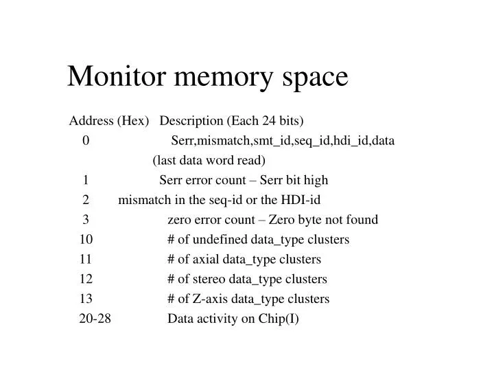
Monitor memory space. Address (Hex) Description (Each 24 bits) 0 Serr,mismatch,smt_id,seq_id,hdi_id,data (last data word read) 1 Serr error count – Serr bit high 2 mismatch in the seq-id or the HDI-id

E N D
Monitor memory space Address (Hex) Description (Each 24 bits) 0 Serr,mismatch,smt_id,seq_id,hdi_id,data (last data word read) 1 Serr error count – Serr bit high 2 mismatch in the seq-id or the HDI-id 3 zero error count – Zero byte not found 10 # of undefined data_type clusters 11 # of axial data_type clusters 12 # of stereo data_type clusters 13 # of Z-axis data_type clusters 20-28 Data activity on Chip(I)
Miscellaneous memory space • The miscellaneous memory space constitutes of - • 1. Bad channel: 32 X 64 – address : 0400 – 047F • 2. Chip ranges : 24 X 1 – address : 0480 • 3. Pulse area thresholds:36 X 4 • – address : 0500 – 0503 • 4. Miscellaneous parameters: 20 X 1 – SEQ_ID(8), HDI_ID(3),Disable bit(1), and Delay count (8). – address : 0580 • 5. Cluster threshold values: 17 X 4 • – address : 0600 – 0603
Approach 1 The synthesis tool was allowed to fit the design in minimum number of FPLDs The synthesis tool mapped the design in five FPLDs such that the Embedded Array Blocks (EABs) were uniformly distributed but the major portion of the memory was set in the larger FPLDs. The FPLDs holding the memory had very small percentage of logic cells occupied.
Approach 2 The Hit Filter and L3 buffers are forced in one FPLD each and the synthesis toolis allowed to fit Strip Reader and Centroid Finder The synthesis tool tries to accommodate some of the excess logic, specially the memory of strip_reader_chip into the FPLD assigned to L3 buffer and very small fraction of it into FPLD assigned to Hit Filter and thus overall design fits into three FPLDs.
Approach 3 The Hit Filter and L3 buffers are forced to fit in one FPLD each and the Strip Reader with Centroid Finder is forced to fit in two FPLDs The strip reader needed two FPLDs because of the need of EABs for the memory blocks. Each memory block regardless of the memory requirement has minimum of two EABs,this is due to the word length more than 8 bits.
Approach 4 - The Hit Filter, L3 buffers and the Strip Reader with Centroid Finder are forced to fit in one FPLD each The strip reader design now fits into one chip , because downloaded parameters do not use EABs