Download
1 / 22
240 likes | 423 Views
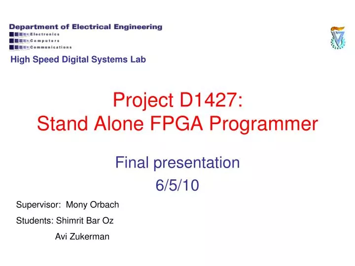
High Speed Digital Systems Lab. Project D1427: Stand Alone FPGA Programmer. Final presentation 6/5/10. Supervisor: Mony Orbach Students: Shimrit Bar Oz Avi Zukerman. Agenda. Project characterization. Technical description. User interface. Blocks diagram.

E N D
High Speed Digital Systems Lab Project D1427:Stand Alone FPGA Programmer Final presentation 6/5/10 Supervisor: Mony Orbach Students: Shimrit Bar Oz Avi Zukerman
Agenda • Project characterization. • Technical description. • User interface. • Blocks diagram. • .hexout format. • Test case. • Work flow summary. • Software. • Hardware. • Schematics. • Implementations Vs. Plan. • Conclusions and summary.
Project characterization • Design a system for programming Altera FPGA directly from a PC. • The system gets gate level burn ready software from PC in hexout format. • Translate to JTAG format. • Burn the software onto an Altera FPGA. FPGA programmer hexout format JTAG format
MMC experiment card DLP Cyclone Driver JTAG output hexout input USB JTAG inputs Technical descriptionInitial plan • The system is uses the MMC experiment card which contains: a DLP Altera Cyclone FPGA. • The system also includes software driver.
User interface • The user interface will be a command line software. • The command line will include the input which is a valid .hexout file. • The software will output success message or failure errors.
Blocks diagramInitial plan acknowledge acknowledge acknowledge • Software block transmits the .hexout file to the DLP. • Receiver block receives the bytes and store it. • Transmitter block transmits the Byte to the target FPGA. transmit transmit Software block Receiver block JTAG output Transmitter block JTAG output hexout Binary Byte Byte
Blocks diagramFinal plan acknowledge acknowledge transmit Software block DLP block JTAG output JTAG output hexout Binary Byte Control • Software block transmits the .hexout file to the DLP. • DLP outputs connect to target FPGA with JTAG interface.
.hexout format • The input to the system should be a completely burn ready program from Quartus.
Test case • The card from the digital system experiment has been chosen as a test case. • The test case is a simple program that changes the card’s display. • The test case had been completed successfully using full Quartus flow and .sof format.
Work flow Summary • Understanding the system requirements and choosing hardware. • Learning the Quartus burn file formats. • HDL designer and Quartus work environment. • The project’s test case had been preformed on full Quartus flow. • Internal blocks interface characterization. • Implementation of software and hardware blocks. • Re characterization of blocks interface after initial implementation. • Implementation of the system with only the software block. • Design of hardware card as replacement to initial plan.
Software • Used C++ to implement the software • The software was divided to several modules: • FTD2XX.dll package for using the USB. • Fpga_load.cpp the main application. • Other support classes. • The software has two main functions: • Parsing the input .hexout file. • Loading the content on the target FPGA byte by byte
Hardware • The main element of the hardware is the DLP used as an interface between the computer’s USB port and the target FPGA JTAG port. • The data between the DLP and target FPGA runs threw two buffers: control buffer and data buffer.
Schematic - JTAG connector • A 15 pin connector as output. • Connecting to standard JTAG connector: • Pin 8 to DCLK • Pin 7 to DATA • Pin 6 to nStatus • Pin 5 to nConfig • Pin 4 to CONF_DONE
Implementations Vs. Plan • Project was implemented in a single software block. • Implemented “dummy” combinational block to act as a feed threw the FPGA. • Designed a specific card for this project. • There was no validation of the code and hardware.
Conclusions and summary • Although we didn’t complete the task of verifying the project we feel we have learned a lot on the different options to burn hardware on FPGA. • The DLP is a powerful unit that can be used to perform almost any task no a PCB card controlled by a computer with a standard USB connection.