Download
1 / 11
110 likes | 200 Views
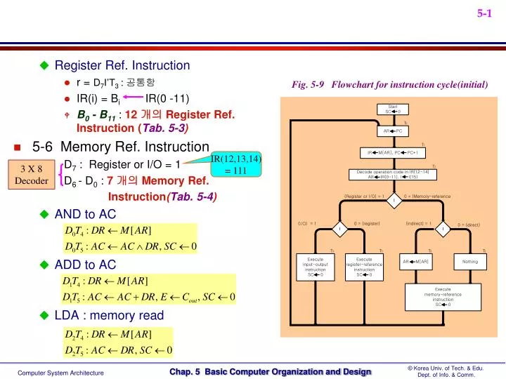
Register Ref. Instruction r = D 7 I’T 3 : 공통항 IR(i) = B i IR(0 -11) B 0 - B 11 : 12 개의 Register Ref. Instruction ( Tab. 5-3 ) 5-6 Memory Ref. Instruction D 7 : Register or I/O = 1 D 6 - D 0 : 7 개의 Memory Ref. Instruction ( Tab. 5-4 ) AND to AC

E N D
Register Ref. Instruction • r = D7I’T3 : 공통항 • IR(i) = Bi IR(0 -11) • B0 - B11 : 12 개의 Register Ref. Instruction (Tab. 5-3) • 5-6 Memory Ref. Instruction D7 : Register or I/O = 1 D6 - D0 : 7 개의 Memory Ref. Instruction(Tab. 5-4) • AND to AC • ADD to AC • LDA : memory read Fig. 5-9 Flowchart for instruction cycle(initial) IR(12,13,14) = 111 3 X 8 Decoder
0 BSA 135 next instruction 21(return address) Subroutine 1 BUN 135 PC = 10 PC = 21 135 PC = 136 • STA : memory write • BUN : branch unconditionally • BSA : branch and save return address • Return Address : save return address ( 135 21 ) • Subroutine Call : Fig. 5-10 • ISZ : increment and skip if zero • Control Flowchart : Fig. 5-11 • Flowchart for the 7 memory reference instruction • The longest instruction : ISZ(T6) • 따라서 3 bit Sequence Counter로 구현가능(현재 4 비트는 확장에 대비함) Fig. 5-10 Example of BSA
5-7 Input-Output and Interrupt • Input-Output Configuration : Fig. 5-12 • Input Register(INPR), Output Register(OUTR) • These two registers communicate with a communication interface serially and with the AC in parallel • Each quantity of information has eight bits of an alphanumeric code • Input Flag(FGI), Output Flag(FGO) • FGI : set when INPR is ready(입력데이터가 있을 때), clear when INPR is empty • FGO : set when operation is completed(데이터 출력 완료), clear when output device is in the process of printing • Input-Output Instruction : Tab. 5-5 • p = D7IT3 : 공통항 • IR(i) = Bi IR(6 -11) • B6 - B11 : 6 개의 I/O Instruction • Program Interrupt • I/O Transfer Modes • 1) Programmed I/O, 2) Interrupt-initiated I/O, 3) DMA, 4) IOP • 본 교과서에서는 2) Interrupt-initiated I/O 방식 사용(FGI 또는 FGO가 1이면 Int. 발생) • Maskable Interrupt 사용( ION 또는 IOF 명령을 사용하여 Int. mask 가능) 1 : Ready 0 : Not ready Address 로 사용되지 않음
256(return address) 0 BUN 1120 Main Program Interrupt Service Routine 1 BUN 0 0 PC = 1 255 256 1120 Interrupt Here • Interrupt Cycle : Fig. 5-13 • During the execute phase, IEN is checked by the control • IEN = 0 : the programmer does not want to use the interrupt, so control continues with the next instruction cycle • IEN = 1 : the control circuit checks the flag bit, If either flag set to 1, R F/F is set to 1 • At the end of the execute phase, control checks the value of R • R = 0 : 보통의 instruction cycle로 들어감 • R = 1 : Instruction cycle로 들어감 • Demonstration of the interrupt cycle : Fig. 5-14 • The memory location at address 0 as the place for storing the return address • Interrupt 발생시 항상 Branch to memory location 1 • Interrupt cycle에서 항상 IEN=0 으로 함(따라서 ISR에서 Interrupt를 받기 위해서는 ISR 앞부분에서 반드시 ION 명령을 실행해야 함) • The condition for R = 1 • Modified Fetch Phase • Modified Fetch and Decode Phase Save Return Address(PC) at 0 Jump to 1(PC=1)
5-8 Complete Computer Description • The final flowchart of the instruction cycle : Fig. 5-15 • The control function and microoperation : Tab. 5-6 • 5-9 Design of Basic Computer • The basic computer consists of the following hardware components • 1. A memory unit with 4096 words of 16bits • 2. Nine registers : AR, PC, DR, AC, IR, TR, OUTR, INPR, and SC(Fig. 2-11) • 3. Seven F/Fs : I, S, E, R, IEN, FGI, and FGO • 4. Two decoder in control unit : 3 x 8 operation decoder, 4 x 16 timing decoder(Fig. 5-6) • 5. A 16-bit common bus(Fig. 5-4) • 6. Control Logic Gates : Fig. 5-6의 오른쪽 Box 부분에서Control Output 설계 • 7. Adder and Logic circuit connected to the AC input • Control Logic Gates • 1. Signals to control the inputs of the nine registers • 2. Signals to control the read and write inputs of memory • 3. Signals to set, clear, or complement the F/Fs • 4. Signals for S2 S1 S0 to select a register for the bus • 5. Signals to control the AC adder and logic circuit 이번 Section에서 설계하는 주요 내용
Register Control : AR • Control inputs of AR : LD, INR, CLR • Find all the statements that change the AR inTab. 5-6 • Control functions • Memory Control : READ • Control inputs of Memory : READ, WRITE • Find all the statements that specify a read operation in Tab. 5-6 • Control function • F/F Control : IEN • Control functions
Bus Control • Encoder for Bus Selection : Tab. 5-7 • S0 = x1 + x3 + x5 + x7 • S1 = x2 + x3 + x6 + x7 • S0 = x4 + x5 + x5 + x7 • x1 = 1 : • Control Function : • x2 = 1 : • x7 = 1 : • Same as Memory Read • Control Function : Encoder Multiplexer Bus Select Input x1 x2 x3 x4 x5 x6 x7 S0 S1 S2 “ “
5-10 Design of Accumulator Logic • Circuits associated with AC : Fig. 5-19 Fig. 5-21 Fig. 2-11 Fig. 5-20
Control of AC : Fig. 5-20 • Find the statement that change the AC : LD CLR INR
Adder and Logic Circuit : Fig. 5-21( 16 bit = 16 개 필요 ) * Fig. 2-11 로 대체 가능 Increment, Clear, Count 기능
Mano Machine • Fig. 5-4 : Common Bus(p.130) • Fig. 2-11 : Register(p. 59) • Fig. 5-6 : Control Unit(p. 137) • Fig. 5-16, 17,18 : Control Logic Gate(p.161- 163) • Fig. 5-4의 모든 Component의 Control Input • 각각의 Register, Memory, F/Fs, Bus Selection • Fig. 5-20 : AC control(p.165) • Fig. 5-21 : Adder and Logic(p.166) Integration ! Due Date : 기말고사 후 1 주일