Download
1 / 3
30 likes | 43 Views
When Cloning Power Supply Circuit Board Gerber File, the layout of the components should be compact, all the connections should be kept as short as possible, and the components and wiring should be laid out according to the functional relationship of the components in the Power Supply Circuit Board schematic diagram

E N D
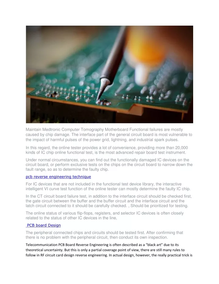
Maintain Medtronic Computer Tomography Motherboard Functional failures are mostly caused by chip damage. The interface part of the general circuit board is most vulnerable to the impact of harmful pulses of the power grid, lightning, and industrial spark pulses. In this regard, the online tester provides a lot of convenience, providing more than 20,000 kinds of IC chip online functional test, is the most advanced repair board test instrument. Under normal circumstances, you can find out the functionally damaged IC devices on the circuit board, or perform exclusive tests on the chips on the circuit board to narrow down the fault range, so as to determine the faulty chip. pcb reverse engineering technique For IC devices that are not included in the functional test device library, the interactive intelligent VI curve test function of the online tester can mostly determine the faulty IC chip. In the CT circuit board failure test, in addition to the interface circuit should be checked first, the gate circuit between the buffer and the buffer circuit and the interface circuit and the latch circuit connected to it should be carefully checked. , Should be prioritized for testing. The online status of various flip-flops, registers, and selector IC devices is often closely related to the status of other IC devices in the line, PCB board Design The peripheral connected chips and circuits should be tested first. After confirming that there is no problem with the peripheral circuit, then conduct its own inspection. Telecommunication PCB Board Reverse Engineering is often described as a “black art” due to its theoretical uncertainty. But this is only a partial coverage point of view, there are still many rules to follow in RF circuit card design reverse engineering. In actual design, however, the really practical trick is
how to compromise these laws when they are not enforceable due to various constraints. Important RF design topics include: impedance and impedance matching, insulation materials and laminates, wavelengths and harmonics…etc. printed circuit boards assembly In the development process of WiFi products, RF circuit layout (RF Circuit Layout Guide) is a very critical process. Many times, we may have perfected the design in principle, but in the actual board making, it is found that it is not ideal after the upper part. In fact, these are the reasons why the layout is not perfect. This article will explain some issues that should be paid attention to in the wiring of the radio frequency circuit based on a wiring example of a wireless network card and a little work experience of mine. Cool that you described the entire project in a 12 letter acronym! Although these documents will provide a general idea of the scope of work, it is likely that the design engineer will ask you many questions, or worse… make a major mistake! While this may seem like an extreme example, it’s a fact of life that I’ve experienced firsthand! PCB board repair After looking at design entry packages for decades, we’ve gotten good pcb board design documents such as schematic diagram, layout drawing, bom list and gerber file, entry packages, bad ones, and downright rubbish. Every printed circuit board cloning, when preparing project documentation, should keep in mind the term “garbage in, garbage out” in pc board layout design. The truth is, more than half of the design entry packages we get are incomplete, lacking circuit performance requirements, incomplete part numbers, and some big holes in the general specification. Power plane copper is the quickest and easiest option for most printed wiring board reverse engineering design software. By sharing a large number of wires, current flow is guaranteed at the highest efficiency with minimal impedance or voltage drop, while providing an adequate return path to ground. If possible, multiple power supply lines can also be run in the same area of the Unmanned Aerial Vehicle PCB Board to confirm whether the ground plane covers most of a certain layer of the PCB, which is conducive to the interaction between the running lines on adjacent layers; For example: placing the discrete components required for the OpAmp operational amplifier close to the device so that the bypass capacitors and resistors can cooperate with it, this helps to optimize the routing length mentioned in the second rule, and also makes the test and fault detection easier; Some chips are inexplicably damaged, mostly due to electrostatic discharge. The general chip antistatic voltage value is 1000V ~ 2000V. The TIL chip is about 1000V, the NMOS chip is about 500V, and the EPROM chip is only about 200V. The static voltage of the human body is generally tens of thousands of volts. Therefore, in the circuit board
maintenance operation, you should pay attention to the use of anti-static bracelets to prevent accidental chip damage. The soldering of the chip is also a problem that can’t be ignored. Otherwise, the faulty chip is found, and it is just that it can’t be replaced. The small wave soldering machine and the tin removal table can easily pick up and solder ordinary IC chips, replace the fixture to remove and solder the surface-mounted gate array chips, etc. It is a higher-level soldering tin removal equipment, but the price is more expensive. More :- How to build a circuit board copy